SiT6502EB HW UM Preliminary Rev 1.0
Page 14 of 33
www.sitime.com
SiT6502EB Evaluation Board (EVB) HW User Manual
VDDS Supply
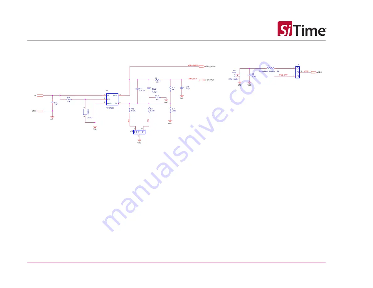
Figure A2. SiT6502EB VDDS Supply Diagram
Страница 1: ...hematic Diagrams 13 Appendix B EVB Top View 32 1 Introduction The SiT6502EB Evaluation Board EVB is designed evaluating the programmable jitter attenuating clock synthesizer SiT95147 device 2 SiT6502EB Features Powered from USB port or external power supply Programmable VDDO supplies for each of the 8 outputs selectable from 3 3 2 5 or 1 8V Status LEDs for power supplies status signals of SiT6502E...
Страница 2: ...al clock signals Outputs SMA connectors J43 through J62 for synthesized clock outputs External FTDI supply 2 pin connector H13 External 3 3V VDD Left Input receiver supply 2 pin connector H1 External 3 3V VDD PLL supply 2 pin connector H12 External Output VDD Supply 2 pin connectors H2 through H11 Common Mode to GND Headers in output terminations 2 pin Headers JSCL13 through JSCL22 Output LDO Regu...
Страница 3: ...y voltage levels switching Header 3 pin Header J9 FTDI supply voltages source switching Header 3 pin Header J78 FTDI supply voltage levels switching Header 3 pin Header J30 USB External Power sources switching Headers 3 pin Headers J79 J6 Outputs supply voltage source switching Header 3 pin Headers J10 J77 J14 J16 J18 J20 J22 J24 J26 J28 Outputs supply voltage levels switching Header 3 pin Headers...
Страница 4: ... J67 3 Pin O JSCL7 2 Pin I J11 3 Pin 1 to 2 J68 3 Pin O JSCL8 2 Pin I J12 2 Pin O J69 3 Pin O JSCL9 2 Pin I J13 3 Pin 1 to 2 J71 3 Pin O JSCL10 2 Pin I J14 3 Pin 1 to 2 J72 3 Pin O JSCL11 2 Pin I J15 3 Pin 1 to 2 J73 3 Pin 1 to 2 JSCL12 2 Pin I J16 3 Pin 1 to 2 J74 3 Pin O JSCL13 2 Pin O J17 3 Pin 1 to 2 J75 3 Pin 2 to 3 JSCL14 2 Pin O J18 3 Pin 1 to 2 J76 10 Pin Header 1 to 2 3 to 4 7 to 8 9 to 1...
Страница 5: ...e 4 lists the Status LEDs on the SiT6502EB EVB in Figure 1 Table 4 SiT6502EB Status LEDs Location Color Status Function Indication D5 Blue 5V Main USB Power D6 Blue 5V Additional USB Power D12 Green FTDI_5V_Power D13 Green FTDI_3 3V_Power Note All LEDs are illuminated when corresponding voltages are present Figure 1 Status LEDs ...
Страница 6: ...ease refer to SiT95147 datasheet for configuring the supply voltages on the VDDIN VDD and VDDOx pins and to the Table 5 for on board configuration options for SiT95147 Table 5 SiT6502EB Supply configuration Variant VDD VDDIN VDDOx SiT95147 2 5V 3 3V 2 5V 3 3V 1 8V 2 5V 3 3V Figure 2 Supply Regulator for VDDIN VDDOx Note For changing the VDDIN J9 and VDDOx Supply connect the corresponding Jumpers t...
Страница 7: ... User Manual Figure 3 External Supply Connection Provision PLLs supply circuitry is shown in Figure 4 Figure 4 Supply Regulator for PLLs Note For changing the VDD J32 Supply connect the Jumper to below settings 1 3 3V Connect the 3 Pin Jumper from 2 to 3 2 2 5V Connect the 3 Pin Jumper from 1 to 2 ...
Страница 8: ... Regulator for PLLs For SPI Mode of Operation 1 SCLK_OUT is shorted to SCLK in J76 2 SDAIO_OUT is shorted to SDAIO in J76 3 CSB_OUT is shorted to CSB in J76 4 SDO_OUT is shorted to SDO in J76 5 JSCL1 Jumper should be removed 6 JVDD1 Jumper should be changed from 2 to 3 to 1 to 2 7 J73 Jumper should be changed from 1 to 2 to 2 to 3 10 Clock Inputs The SiT6502EB has eight inputs 4 differential pairs...
Страница 9: ...pairs Figure 6 Input Clock Termination Circuit 11 Clock Outputs When shipped from factory each of the twenty output drivers 8 differential pairs is ac coupled to its respective SMA connector this is the default configuration The output clock termination circuit is shown in Figure 7 below If dc coupling is required the corresponding 0 1 uF ac coupling capacitor can be replaced with a zero resistor ...
Страница 10: ...instead of the corresponding series resistors RSExx Refer to Table 6 which are not populated Table 6 Output Port RSExx Resistors Output Port 0 1 2 3 4 5 6 7 0B 0T 0 1 uF capacitors RSE1 RSE5 RSE2 RSE6 RSE4 RSE7 RSE3 RSE8 RSE10 RSE14 RSE9 RSE13 RSE11 RSE15 RSE12 RSE16 RSE17 RSE19 RSE18 RSE20 Output termination resistors as shown in Table 7 are not populated CSE6 10pF VCM_1 JSCL14 JSCL2 1 2 DNP J44 ...
Страница 11: ...D 3 3V 150 150 150 150 150 150 150 150 150 150 VDD 2 5V 120 120 120 120 120 120 120 120 120 120 Also ensure that jumpers JSCLxx as per Table 9 are populated to allow path to GND Table 9 Output Port Jumpers to GND Output Port 0 1 2 3 4 5 6 7 0B 0T Jumpers to GND JSCL13 JSCL14 JSCL15 JSCL16 JSCL17 JSAL18 JSCL19 JSCL20 JSCL21 JSCL22 11 1 3 HCSL For HCSL output configuration series resistors RSExx Ref...
Страница 12: ...ation is shown in Figure 8 Figure 8 SiT6502EB Starter Connection Diagram The general guidelines for single USB power supply operation are listed below Use either a USB 3 0 or USB 2 0 port These ports are specified to supply 900 mA and 500 mA respectively at 5V If you are working with a USB 2 0 port and you are current limited turn off enough DUT output voltage regulators to drop the total DUT curr...
Страница 13: ...iT6502EB HW UM Preliminary Rev 1 0 Page 13 of 33 www sitime com SiT6502EB Evaluation Board EVB HW User Manual Appendix A EVB Schematic Diagrams EVB Top Level Diagram Figure A1 SiT6502EB Top Level Diagram ...
Страница 14: ...SiT6502EB HW UM Preliminary Rev 1 0 Page 14 of 33 www sitime com SiT6502EB Evaluation Board EVB HW User Manual VDDS Supply Figure A2 SiT6502EB VDDS Supply Diagram ...
Страница 15: ...SiT6502EB HW UM Preliminary Rev 1 0 Page 15 of 33 www sitime com SiT6502EB Evaluation Board EVB HW User Manual Power Supply Figure A3 SiT6502EB Power Supply Diagram ...
Страница 16: ...SiT6502EB HW UM Preliminary Rev 1 0 Page 16 of 33 www sitime com SiT6502EB Evaluation Board EVB HW User Manual Left Supply Figure A4 SiT6502EB Left Supply Diagram ...
Страница 17: ...SiT6502EB HW UM Preliminary Rev 1 0 Page 17 of 33 www sitime com SiT6502EB Evaluation Board EVB HW User Manual ODR1 Supply Figure A5 SiT6502EB ODR1 Supply Diagram ...
Страница 18: ...SiT6502EB HW UM Preliminary Rev 1 0 Page 18 of 33 www sitime com SiT6502EB Evaluation Board EVB HW User Manual ODR2 Supply Figure A6 SiT6502EB ODR2 Supply Diagram ...
Страница 19: ...SiT6502EB HW UM Preliminary Rev 1 0 Page 19 of 33 www sitime com SiT6502EB Evaluation Board EVB HW User Manual ODR3 Supply Figure A7 SiT6502EB ODR3 Supply Diagram ...
Страница 20: ...SiT6502EB HW UM Preliminary Rev 1 0 Page 20 of 33 www sitime com SiT6502EB Evaluation Board EVB HW User Manual ODR5 Supply Figure A8 SiT6502EB ODR5 Supply Diagram ...
Страница 21: ...SiT6502EB HW UM Preliminary Rev 1 0 Page 21 of 33 www sitime com SiT6502EB Evaluation Board EVB HW User Manual ODR6 Supply Figure A9 SiT6502EB ODR6 Supply Diagram ...
Страница 22: ...SiT6502EB HW UM Preliminary Rev 1 0 Page 22 of 33 www sitime com SiT6502EB Evaluation Board EVB HW User Manual ODR7 Supply Figure A10 SiT6502EB ODR7 Supply Diagram ...
Страница 23: ...SiT6502EB HW UM Preliminary Rev 1 0 Page 23 of 33 www sitime com SiT6502EB Evaluation Board EVB HW User Manual ODR0B Supply Figure A11 SiT6502EB ODR0B Supply Diagram ...
Страница 24: ...SiT6502EB HW UM Preliminary Rev 1 0 Page 24 of 33 www sitime com SiT6502EB Evaluation Board EVB HW User Manual ODR0T Supply Figure A12 SiT6502EB ODR0T Supply Diagram ...
Страница 25: ...SiT6502EB HW UM Preliminary Rev 1 0 Page 25 of 33 www sitime com SiT6502EB Evaluation Board EVB HW User Manual FTDI Supply Figure A13 SiT6502EB FTDI Supply Diagram ...
Страница 26: ...SiT6502EB HW UM Preliminary Rev 1 0 Page 26 of 33 www sitime com SiT6502EB Evaluation Board EVB HW User Manual PLL Supply Figure A14 SiT6502EB PLL Supply Diagram ...
Страница 27: ...SiT6502EB HW UM Preliminary Rev 1 0 Page 27 of 33 www sitime com SiT6502EB Evaluation Board EVB HW User Manual INPUT CLKS Figure A15 SiT6502EB INPUT CLKS Diagram ...
Страница 28: ...SiT6502EB HW UM Preliminary Rev 1 0 Page 28 of 33 www sitime com SiT6502EB Evaluation Board EVB HW User Manual OUTPUT CLKS Figure A16 SiT6502EB OUTPUT CLKS Diagram ...
Страница 29: ...SiT6502EB HW UM Preliminary Rev 1 0 Page 29 of 33 www sitime com SiT6502EB Evaluation Board EVB HW User Manual STATUS LEDS 2 Figure A17 SiT6502EB STATUS LEDS 2 ...
Страница 30: ...SiT6502EB HW UM Preliminary Rev 1 0 Page 30 of 33 www sitime com SiT6502EB Evaluation Board EVB HW User Manual QFN SiT95147 EVB Figure A18 QFN SiT95147 EVB Diagram ...
Страница 31: ...SiT6502EB HW UM Preliminary Rev 1 0 Page 31 of 33 www sitime com SiT6502EB Evaluation Board EVB HW User Manual FTDI Figure A19 SiT6502EB FTDI Diagram ...
Страница 32: ... Page 32 of 33 www sitime com SiT6502EB Evaluation Board EVB HW User Manual Appendix B EVB Top View Figure A20 SiT6502EB Top View USB Cable from PC IN1 IN0 IN3 CLK7_OUT CLK6_OUT CLK5_OUT CLK3_OUT CLK2_OUT CLK0T_OUT CLK1_OUT CLK0B_OUT IN2 ...
Страница 33: ... merchantability and fitness for use or a particular purpose and any implied warranty arising from course of dealing or usage of trade as well as any common law duties relating to accuracy or lack of negligence with respect to this material any SiTime product and any product documentation Products sold by SiTime are not suitable or intended to be used in a life support application or component to ...