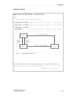
The solution
Consecutive data words of a DB or DX data block are defined from
DW 0 onwards as "IPC data words". Each link is assigned its own
data block and is totally independent of the other links.
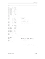
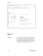
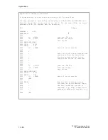
At the beginning of the cycle block, the IPC data words are received with
the aid of the special function organization blocks for multiprocessor
communication. This is followed by the "regular" cyclic program, that
evaluates the received data and generates the data to be sent. At the end
of the cycle, this data is then sent with the aid of the special organization
blocks for multiprocessor communication. It can therefore be received by
the other CPUs at the beginning of their cycles.
The following applies for each of the maximum 12 possible links
regardless of the other links:
••
The transmitting CPU is only active when the receiving CPU has
read out all the "old" data from the COR 923C buffer.
••
The receiving CPU is only active when the transmitting CPU has
written all the "new" data in the COR 923C buffer.
This means that the receiving CPU can either receive a complete new
data record or the old data record remains unchanged: no mixing of
"old" and "new" data.
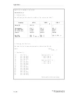
Data structure
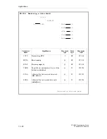
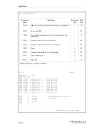
Which data words (for the data word area below) are to be transferred
from which CPU to which CPU is described in the link list (see the table
on the following page). This is located in an additional data block that
must exist in all the CPUs involved.
The data word areas always begin from data word DW 0, and their
lengths are specified in data fields. Remember the following points:
••
A complete data field consists of 32 data words.
••
If the last data field is "truncated", i.e. it contains between 1 and 31
data words, less data words are transferred.
••
If a send data block is longer than the number of fields of data
specified in the link list, the excess data words can be used in the
corresponding CPU.
••
If a receive data block is longer than the received data word area,
the excess data words can be used in the corresponding CPU.
Applications
CPU 948 Programming Guide
C79000-G8576-C848-04
10 - 67
Содержание CPU 948
Страница 10: ...Contents CPU 948 Programming Guide 1 2 C79000 G8576 C848 04 ...
Страница 32: ...Contents CPU 948 Programming Guide 2 2 C79000 G8576 C848 04 ...
Страница 72: ...Data Blocks CPU 948 Programming Guide 2 42 C79000 G8576 C848 04 ...
Страница 74: ...Contents CPU 948 Programming Guide 3 2 C79000 G8576 C848 04 ...
Страница 154: ...Contents CPU 948 Programming Guide 4 2 C79000 G8576 C848 04 ...
Страница 200: ...Contents CPU 948 Programming Guide 5 2 C79000 G8576 C848 04 ...
Страница 308: ...Contents CPU 948 Programming Guide 7 2 C79000 G8576 C848 04 ...
Страница 324: ...Examples of Parameter Assignment CPU 948 Programming Guide 7 18 C79000 G8576 C848 04 ...
Страница 326: ...Contents CPU 948 Programming Guide 8 2 C79000 G8576 C848 04 ...
Страница 370: ...Addressable System Data Area CPU 948 Programming Guide 8 46 C79000 G8576 C848 04 ...
Страница 372: ...Contents CPU 948 Programming Guide 9 2 C79000 G8576 C848 04 ...
Страница 404: ...Operations with the Base Address Register BR Register CPU 948 Programming Guide 9 34 C79000 G8576 C848 04 ...
Страница 486: ...Contents CPU 948 Programming Guide 11 2 C79000 G8576 C848 04 ...
Страница 522: ...PG Functions via the S5 Bus CPU 948 Programming Guide 11 38 C79000 G8576 C848 04 ...
Страница 524: ...Contents CPU 948 Programming Guide 12 2 C79000 G8576 C848 04 ...
Страница 538: ...Contents CPU 948 Programming Guide 13 2 C79000 G8576 C848 04 ...
Страница 546: ...List of Key Words CPU 948 Programming Guide Index 6 C79000 G8576 C848 04 ...

