
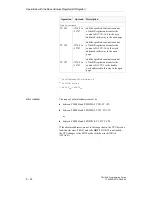


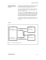


2. Type in the individual operand areas (from data word 3 onwards).
Before each operand area, you must specify an ID. The possible ID
words are as follows:
ID word for digital inputs
KH = DE00
ID word for digital outputs
KH = DA00
ID word for IPC input flags
KH = CE00
ID word for IPC output flags
KH = CA00
After each ID word, use fixed-point format to list the numbers of the
inputs and outputs used.
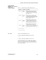
3. Complete the entries with the DB 1 end ID "KH = EEEE" and
transfer DB 1 to the CPU.
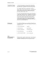
Note
You can make the DB 1 entries in any order. Remember that the
process image of the inputs and outputs is updated in the reverse
order to which you store the addresses in DB 1 (i.e. the last entry
is updated first).
Multiple entries of the same bytes (e.g., for test purposes) are
possible. The system program makes multiple updates of the process
images of bytes that are entered more than once.
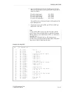
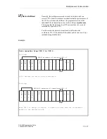
Example of editing DB 1
DB1
FD: CPU948ST.S5D
0:
KH = 4D41;
DW 0-2:
1:
KH = 534B;
Start ID
2:
KH = 3031;
for DB 1
3:
KH = DE00;
ID word for digital inputs
4:
KF = +00000;
Input byte 0
5:
KF = +00001;
Input byte 1
6:
KF = +00002;
Input byte 2
7:
KF = +00003;
Input byte 3
8:
KF = +00007;
.
9:
KF = +00010;
Input byte 10
10:
KH = DA00;
ID word for digital outputs
11:
KF = +00000;
Output byte 0
12:
KF = +00002;
Output byte 2
13:
KF = +00004;
.
14:
KF = +00012;
Output byte 12
15:
KH = CE00;
ID word for IPC flag inputs
16:
KF = +00050;
Flag byte 50
17:
KF = +00051;
.
18:
KF = +00060;
Flag byte 60
19:
KH = CA00;
ID word for IPC flag outputs
20:
KF = +00070;
Flag byte 70
21:
KF = +00072;
.
22:
KF = +00100;
Flag byte 100
23:
KH = EEEE;
End ID
24:
Multiprocessor Mode
CPU 948 Programming Guide
C79000-G8576-C848-04
10 - 11
Содержание CPU 948
Страница 10: ...Contents CPU 948 Programming Guide 1 2 C79000 G8576 C848 04 ...
Страница 32: ...Contents CPU 948 Programming Guide 2 2 C79000 G8576 C848 04 ...
Страница 72: ...Data Blocks CPU 948 Programming Guide 2 42 C79000 G8576 C848 04 ...
Страница 74: ...Contents CPU 948 Programming Guide 3 2 C79000 G8576 C848 04 ...
Страница 154: ...Contents CPU 948 Programming Guide 4 2 C79000 G8576 C848 04 ...
Страница 200: ...Contents CPU 948 Programming Guide 5 2 C79000 G8576 C848 04 ...
Страница 308: ...Contents CPU 948 Programming Guide 7 2 C79000 G8576 C848 04 ...
Страница 324: ...Examples of Parameter Assignment CPU 948 Programming Guide 7 18 C79000 G8576 C848 04 ...
Страница 326: ...Contents CPU 948 Programming Guide 8 2 C79000 G8576 C848 04 ...
Страница 370: ...Addressable System Data Area CPU 948 Programming Guide 8 46 C79000 G8576 C848 04 ...
Страница 372: ...Contents CPU 948 Programming Guide 9 2 C79000 G8576 C848 04 ...
Страница 404: ...Operations with the Base Address Register BR Register CPU 948 Programming Guide 9 34 C79000 G8576 C848 04 ...
Страница 486: ...Contents CPU 948 Programming Guide 11 2 C79000 G8576 C848 04 ...
Страница 522: ...PG Functions via the S5 Bus CPU 948 Programming Guide 11 38 C79000 G8576 C848 04 ...
Страница 524: ...Contents CPU 948 Programming Guide 12 2 C79000 G8576 C848 04 ...
Страница 538: ...Contents CPU 948 Programming Guide 13 2 C79000 G8576 C848 04 ...
Страница 546: ...List of Key Words CPU 948 Programming Guide Index 6 C79000 G8576 C848 04 ...