


– 89 –
SD-CX1W
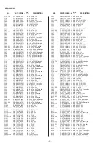
IC1 VH+-1: Focus/Tracking/Spin/Sled Driver (LA6558)
Pin No.
Function
Terminal Name
1*
VO3-
CH3 (-) output.
2*
VO3+
CH3 (+) output.
3
VO5-
CH5 (-) output. Inversion against input.
4
VO5+
CH5 (+) output. Non-inversion against input.
5
VO4-
CH4 (-) output. Inversion against input.
6
VO4+
CH4 (+) output. Non-inversion against input.
7
P-GND
Power system GND (CH3, 4, 5).
8
S-GND
Signal system GND.
9
VREF
Reference voltage input.
10
IN-MUTE
BTL AMP (CH1, 2, 4, 5) and 3.3 V, 5 VREG output. ON/OFF (“H”: Output ON, “L”: Output OFF).
11*
0-RESET
Reset output (open collector).
12
VIN4
CH4 input.
13
VIN5
CH5 input.
14
VIN3+
CH3 input +.
15
VIN3-
CH3 input –.
16
5VERG
5V power output.
17
VIN6-
CH6 input –.
18
VIN6+
CH6 input +.
19
VIN2
CH2 input.
20
VIN1
CH1 input.
21
S-VCC
Signal system VCC.
22
3.3VREG
3.3 V power output.
23
P-VCC
Power system power supply.
24
P-GND2
Power system GND (CH1, 2, 6).
25
V01-
CH1 (-) output. Inversion against input.
26
V01+
CH1 (+) output. Non-inversion against input.
27
V02-
CH2 (-) output. Inversion against input.
28
V01+
CH2 (+) output. Non-inversion against input.
29
V06-
CH6 (-) output.
20
V06+
CH6 (+) output.
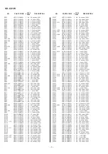
Figure 89 BLOCK DIAGRAM OF IC
In this unit, the terminal with asterisk mark (*) is (open) terminal which is not connected to the outside.
VO3–
VO3+
VO5–
VO5+
VO4–
VO4+
P-GND1
S-GND
VREF
IN-MUTE
0-RESET
VIN4
VIN5
VIN3+
VIN3–
VIN6–
5VREG
VIN6+
VIN2
VIN1
S-VCC(IN)
3.3VREG
(OUT)
P-VCC(IN)
P-GND2
VO1–
VO1+
VO2–
VO2+
VO6–
VO6+
X3/8
X3/8
X3/8
X3/8
22k
22k
22k
22k
200
200
200
200
MUTE
RESET
3.3VREG
5VREG
1
2
3
4
5
6
7
8
9
10
11
12
13
14
15
16
17
18
19
20
21
22
23
24
25
26
27
28
29
30
+
+
–
–
+
–
+
–
+
–
Level
shift
Level
shift
X2
X2
X2
X2
Level shift
Level shift
Level shift
Level shift
Power GND
Signal GND
Standard
voltage
In less than
VREF 0.7V,
RESET output L
BTL-AMP OFF
Power VCC
Signal
VCC
Power GND
Heating
protection circuit
(Thermal shutdown)
Содержание SD-CX1W(BL)
Страница 56: ...SD CX1W 56 Figure 56 WIRING SIDE OF P W BOARD 3 13 A B C D E F G H 1 2 3 4 5 6 TUNER PWB A2 TOP VIEW ...
Страница 114: ...SD CX1W 15 M E M O ...
Страница 115: ...SD CX1W 16 M E M O ...


