background image

CD-DD4500

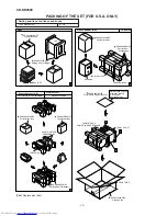
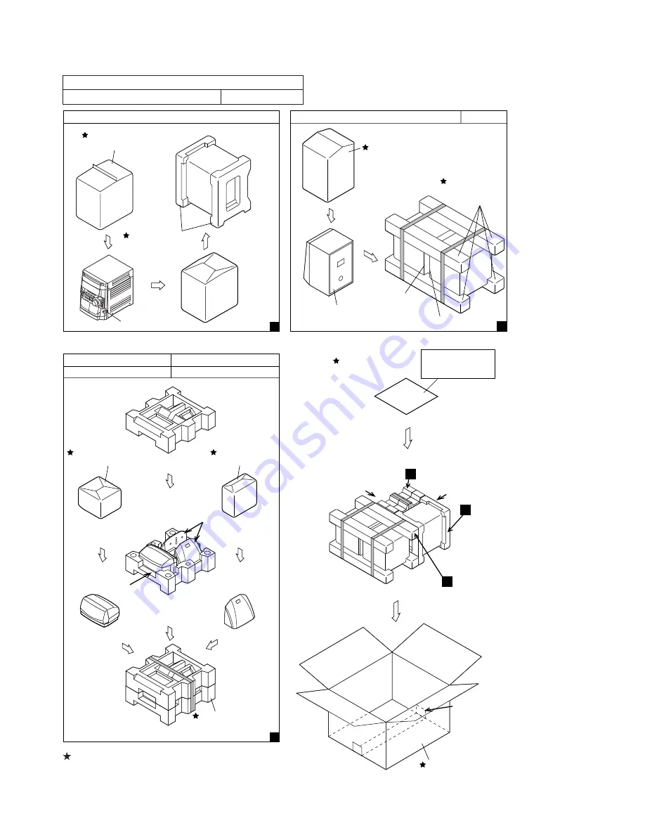
PACKING OF THE SET (FOR U.S.A. ONLY)

Setting position of switches and knobs

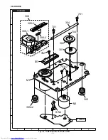
Tape Mechanism

STOP

UNIT

SPAKP0032AWZZ

Polyethylene bag

SPAKA0325AWZZ

Packing Add.,(Left/Right)

IDEAL TAPE

Bottom

REAR SIDE

FRONT-SP(L) TOP

FRONT-SP(R) TOP

TOP

FRONT

REAR

1

SSAKH0066AWZZ

Polyethylene Bag

SSAKH0067AWZZ

Polyethylene Bag

PACK TOGETHER

SURROUND-SP

CENTER-SP

SSAKA0315AWZZ

Packing Add.(Top/Bottom)

3

Center Speaker

Surround Speaker (L/R)

GBOXS4008AWM1/GBOXS2008AWM1

GBOXS0064AWM1

SSAKA0007AWZZ

Polyethylene Bag,Accessories

FRONT OF SET

FRONT SIDE

FRONT SIDE OF

CENTER IN REAR SPEAKER

2

1

3

SPAKC1264AWZZ

Packing Case

TOP

Front Speaker (L/R)

CP-DD4500

SPAKA0314AWZZ

Packing Add.,

(Top/Bottom)

SSAKH0053AWZZ

Polyethylene Bag

2

AM/FM Loop Antenna
Operation Manual
Quick Guide
Remote Control

Not Replacement Item

– 15 –

Содержание CD-DD4500

Страница 1: ... COMPONENT SYSTEM MODEL CD DD4500 In the interests of user safety the set should be restored to its original condition and only parts identical to those specified be used SERVICE MANUAL This document has been published to be used for after sales service only The contents are subject to change without notice SHARP CORPORATION CD DD4500 Mini Component System consisting of CD DD4500 main unit CP DD45...

Страница 2: ... Weight 1 3 lbs 0 6 kg each FOR A COMPLETE DESCRIPTION OF THE OPERATION OF THIS UNIT PLEASE REFER TO THE OPERATION MANUAL Specifications for this model are subject to change without prior notice SPECIFICATIONS CD DD4500 CP DD4500 IMPORTANT SERVICE NOTES FOR U S A ONLY BEFORE RETURNING THE AUDIO PRODUCT Fire Shock Hazard Before returning the audio product to the user perform the following safety ch...

Страница 3: ...n 27 Tape 2 Record Pause Button 28 CD Fast Reverse Tape 2 Rewind or Tuner Preset Down Button 5 6 7 1 2 3 4 9 10 11 12 19 23 18 17 16 15 14 13 25 26 27 28 24 20 21 22 8 Display 1 Left Front Speaker Indicator 2 Low Frequency Effect Indicator 3 Center Speaker Indicator 4 Right Front Speaker Indicator 5 Subwoofer Indicator 6 Left Surround Speaker Indicator 7 Surround Indicator 8 Right Surround Speaker...

Страница 4: ...Button 10 CD Stop Button 11 Tape 2 Record Pause Button 12 Tuner Band Button 13 CD Button 14 Extra Bass Button 15 CD Clear Button 16 Power Button 17 Surround Effect Buttons 18 Equalizer Mode Select Button 19 CD Play or Repeat Button 20 CD Fast Forward Preset Up Button 21 Tape 1 Tape 2 Play Button 22 Tape 1 Tape 2 Stop Button 23 Tape 2 Fast Forward Button 24 Tape 2 Rewind Button 25 DVD VCR Button 26...

Страница 5: ... Subwoofer 4 Speaker Wire for SUBWOOFER Terminals 5 Bass Reflex Duct 6 Speaker Wire for MAIN Terminals Front speaker left Front speaker right 2 1 3 2 1 3 4 5 6 4 5 6 2 1 2 1 1 Full Range Speaker 2 Speaker Wire 1 Full Range Speaker 2 Speaker Wire 2 1 GBOXS0064AWM1 GBOXS2008AWM1 GBOXS4008AWM1 ...

Страница 6: ...me in 5 minute intervals The hour will not advance even if minutes advance from 59 to 00 The clock begins counting from 0 seconds Seconds are not displayed The time display will disappear after a few seconds Note that this can only be set when the unit is first installed or it has been reset When you connect this unit to a DVD player which is playing a disc with the trademark you can enjoy realist...

Страница 7: ...ly Sound skipping Cannot hear treble Sound fluctuation Cannot remove the tape Possible cause Is the erase protection tab removed Is it a normal tape You cannot record on a metal or CrO2 tape Is there any slack Is the tape stretched Are the capstans pinch rollers or heads dirty If a power failure occurs during playback the heads remain engaged with the tape Do not open the compartment forcibly Wait...

Страница 8: ... AC power plug from the AC outlet 2 Make sure that the unit vent is not blocked 3 Make sure that the speaker wires have been correctly connected to the speaker terminals 4 After checking items 2 and 3 above wait for 2 or 3 hours before trying to use the unit 5 Reconnect the AC power cord Note If the TIMER indicator flashes again during use please unplug the AC power plug and contact a SHARP author...

Страница 9: ...cover as shown Extraiga la cubierta Inserte las pilas Vuelva a colocar la de las pilas como se muestra cubierta 2 System Connections Conexiones del sistema 3 AC outlet AC 120 V 60 Hz A un tomacorriente de CA 120 V de CA 60 Hz Front speaker Right Altavoz delantero Derecho Front speaker Left Altavoz delantero Izquierdo FM antenna Antena de FM AM loop antenna Antena de cuadro de AM Blue Azul Red Rojo...

Страница 10: ...ntral Front right Delantero derecho Surround left Sonido perimétrico izquierdo Surround right Sonido perimétrico derecho Same distance Misma distancia Front left Delantero izquierdo Center Central Front right Delantero derecho Example When installed on the wall Ejemplo Cuando se instalan en la pared Surround speaker Altavoz de sonido perimétrico Wall Pared 23 5 8 35 7 16 60 90 cm 60 90 cm Example ...

Страница 11: ... de una cinta de cassette TAPE 1 o TAPE 2 Listening to the Radio Audición de la radio TAPE 1 TAPE 2 FM stereo mode indicator Indicador del modo de FM en estéreo FM stereo receiving indicator Indicador de recepción de FM en estéreo 1 Press the TUNER BAND button repeat edly to select the desired frequency band FM or AM Pulse repetidamente el botón TUNER BAND para seleccionar la banda de frecuencia d...

Страница 12: ...xcellent performance 1 Take cassette tape and compact disc out of the unit 2 Be sure to remove the power supply plug from the wall outlet before starting to disassemble the unit 3 Take off nylon bands or wire holders where they need to be removed when disassembling the unit After servicing the unit be sure to rearrange the leads where they were before disassembling 4 Take sufficient care on static...

Страница 13: ...x 1 Power PWB F3 x 2 F3 x 1 F3 x 1 F1 x 1 ø3 x 10mm F3 x 1 Main PWB Amp B PWB Dolby PWB E2 x 1 D2 x 2 C4 x 1 E1 x 9 ø3 x 10mm Rear Panel D1 x 1 ø3 x 10mm D1 x 4 ø3 x 10mm J3 x 1 J2 x 13 ø3 x 10mm K1 x 5 ø3 x 10mm J1 x 1 Display PWB Headphones PWB Open Cassette Holder Tape Mechanism L1 x 1 ø3 x 10mm Lug Wire Washer H1 x 3 ø3 x 8mm Headphones PWB G2 x 1 Amp A PWB Amp B PWB Front Panel G1 x 2 ø3 x 6m...

Страница 14: ...14 1 1 3 2 N1 x 3 N1 x 3 CD Player Unit C1 x 2 ø3 x 10mm Woofer Subwoofer Tweeter A2 x 4 ø4 x 16mm B1 x 4 ø4 x 16mm 1 Subwoofer 1 Front Panel A1 x1 14 4 2 Screw A2 x4 14 5 2 Woofer 1 Screw B1 x4 14 5 3 Tweeter 1 Screw C1 x2 14 5 STEP REMOVAL PROCEDURE FIGURE Figure 14 4 CP DD4500 Screwdriver Driver should be pried away from Speaker Box A1 x 1 Speaker Box ...

Страница 15: ...n of the arrow B Note When installing the pinch roller pay attention to the spring mounting position How to remove the belt TAPE 2 See Fig 15 4 1 Remove the main belt D1 x 1 pc from the motor side 2 Remove the FF REW belt D2 x 1 pc How to remove the belt TAPE 1 See Fig 15 4 1 Remove the main belt E1 x 1 pc from the motor side 2 Remove the FF REW belt E2 x 1 pc How to remove the motor See Fig 15 5 ...

Страница 16: ...onnector so as to protect the optical pickup from electrostatic damage Figure 16 2 CD MECHANISM SECTION Perform steps 1 2 3 12 13 14 and 15 of the disassembly method to remove the CD mechanism How to remove the loading motor See Fig 16 1 1 Bend the hooks A1 x 5 pcs to remove the loading motor 2 Remove the drive belt A2 x 1 pc Figure 16 1 A1 x 2 A1 x 1 Loading Motor Loading Motor PWB Slide Chassis ...

Страница 17: ...ency 400 Hz 30 AM modulation FM mute level adjustment Frequency Adjusting object Adjusting method 98 0 MHz 26 dB EMF VR351 Input CNP301 Output Speaker Terminal FM signal oscillator Frequency 1 kHz 22 5 kHz Adjusting object Preset No Frequency Figure 17 2 FM Mute Level Table 17 Electronic Voltmeter GND AM Loop Antenna AM signal oscillator Loop Antenna UNIT IF Speaker Terminal Frequency cover TP301 ...

Страница 18: ...ons readjustment is not needed when replacing the pickup Therefore different PWBs and pickups can be combined freely Each time a disc is changed these adjustments are performed automatically Therefore playback of each disc can be performed under optimum conditions T T EFBL FDO TE Stopped CH1 500 mV DC 10 1 CH2 200 mV DC 10 1 CH3 1 V DC 10 1 500 ms div 500 ms div NORM 20 kS s 1 2 3 Record Length Sm...

Страница 19: ...y input Tracking OFF play at that specific point MEMORY key input Tracking ON play from that specific point STOP key input STOP IL isn t done VOL Last memory BAL CENTER P GEQ FLAT X BASS OFF To cancel Power OFF Sliding the PICKUP with button must only be in STOP mode MEMORY key input Adjustment result automatically will display as below for each 2 sec a FOFF_XX b TOFF_XX c TBAL_XX d TGAN_XX f FGAN...

Страница 20: ...Current Detection DC Detection TAPE Mechanism Error ER TA 00 Tape Mechanism Error 01 Initial Error 02 03 CD VCD Pickup Mechanism Error ER CD 00 Pickup Mechanism Error 01 PU IN SW Detection NG 02 03 04 CD Changer Mechanism Error ER CD 10 Changer Error 11 Initial Error 12 13 Tray Error ET CD 20 Tray Error 21 22 23 Focus Not Match NO DISC IL Time Over NOT READ TUN PLL Unlock ER TU 00 TUN Error 01 PLL...

Страница 21: ...LVDD ADAVDD RFVDD XL1 33 8688 MHz OC DISC NO CLAMP SW CD RES CLK DI DO CE DRF WRQ 5V B5 5V B5 DGND L CH AGND VCC3 VCC2 VCC4 VCC1 IC2 M63001FP FOCUS TRACKING SPIN SLED DRIVER XIN XOUT RES WRQ DO DI CLK CE TIN2 TIN1 FIN2 FIN1 TD0 FD0 SPDO SLDO CONT5 CONT5 BI7 CONT2 CONT3 CONT4 RCHO RVSS LVSS LCHO 80 42 79 75 20 5 40 18 24 23 14 8 21 22 29 35 41 47 46 7 10 9 8 7 15 1 2 1 2 17 25 42 41 83 39 4 7 6 5 1...

Страница 22: ...B4 B5 B5 B5 16 10 15 14 11 9 3 23 P B REC AC BIAS RECORD PLAYBACK HEAD ERASE HEAD TAPE 2 PLAYBACK HEAD TAPE 1 L CH R CH L CH R CH BIAS OSC Q128 L104 BIAS Q126 Q101 Q102 Q121 Q122 SWITCHING Q124 L103 SWITCHING MUTING IC101 PLAYBACK AND RECORD PLAYBACK AMP PB R L REC REC R L L NF R NF ALC REC T1 T2 T1 T2 NOR HIGH REF R REC L REC POP REDUCE R NF L NF L T2 R T2 R T1 L T1 1 24 2 23 3 22 6 9 16 14 12 15...

Страница 23: ...POWER SUPPLY CORD F801 6 3A 125V T801 MAIN POWER TRANSFORMER T802 SUB POWER TRANSFORMER F804 6 3A 125V F802 4A 125V F803 4A 125V F805 6 3A 125V F806 2A 125V F807 2A 125V IC851 KIA7805AP CONSTANT VOLTAGE REGULATOR IC850 KIA7810AP VOLTAGE REGULATOR IC880 KIA7805AP CONSTANT VOLTAGE REGULATOR B6 5V B4 A_ 10V B3 M_ 12V B5 5V VF1 VF2 VF B1 B2 B1 B2 IC401 STK40224 POWER AMP IC901 STK40270N POWER AMP IC90...

Страница 24: ...RFMON TE TEC FE TIN2 F TIN1 E FIN2 B FIN1 A RSVSS RFVDD RF EFMIN SLCIST SLCO 5 3 6 2 7 1 4 CD MOTOR PWB G GND FO PICKUP UNIT TR TR TR TR FO FO FO PD VR LD F C B A E VCC VREF SLIDE SPIN PU IN 1 2 3 4 5 6 1 2 3 4 5 6 5 3 6 2 7 1 4 5 3 6 2 7 1 4 5 3 6 2 7 1 4 4 1 3 6 5 2 M M 4 8 5 2 1 7 3 6 4 8 5 2 1 7 3 6 4 8 5 2 1 7 3 6 IC2 M63001FP LDD LDS CT1 0 001 CT2 0 001 R65 3 3K C49 47 25 C50 22P CH C12 100P...

Страница 25: ...F1 VREF ADAVSS ADAVDD JITTC RFMON TE TEC FE TIN2 F TIN1 E FIN2 B FIN1 A RSVSS RFVDD RF EFMIN SLCIST SLCO 9 8 7 6 2 4 5 3 1 9 8 7 6 2 4 5 3 1 1 2 3 4 8 6 5 7 9 M 3 5 4 2 6 1 3 5 4 2 6 1 CD LOADING MOTOR PWB E CNP501 TO DOLBY PWB P32 1 B CNS606 FROM MAIN PWB P26 6 H CNS703 BI703 FROM DISPLAY PWB P29 7 H 1 3 2 9 LDD LDS DO DI CL CE C16 10 16 CNP7 C51 0 022 C19 15P C20 15P C36 2 2 50 C48 0 022 C44 0 0...

Страница 26: ...N R196 4 7K R195 1K R194 1K R193 100 R192 1K CNP7 C197 0 015 C194 0 33 R668 10K R667 10K R666 10K R665 10K R109 270K R108 270K R134 68K R107 1K Q101 KRC104 M R110 33K C R179 10K R176 10K R177 10K R178 10K R180 10K BI606 CNS606 C190 0 022 C189 0 022 D184 DS1SS133 D183 DS1SS133 C187 0 022 C186 0 022 D181 DS1SS133 D182 DS1SS133 C602 0 022 C623 10 50 R605 3 9K C605 0 1 C601 100 16 C626 100P CH C604 10...

Страница 27: ...60 10K Q851 KTC2026 Y R892 2 2K R891 2 2K R894 1K Q892 KTC3199 GR R893 1K Q891 KTC3199 GR C892 0 001 C891 0 001 R895 2 2K Q893 KTC3199 GR C893 0 001 R896 1K R196 4 7K R195 1K R194 1K R193 100 R192 1K C858 0 047 ML CNP601 FFC701 CNP701 NP7 RP851 C852 4700 16 C197 0 015 C199 0 0082 C198 0 015 C195 0 33 C194 0 33 R668 10K R667 10K R666 10K R665 10K CNP607 R175 10K R174 10K R173 4 7K R172 4 7K R171 4 ...

Страница 28: ...0K VCC 8 7 6 5 4 3 2 1 MOT_CNT 8 7 6 5 4 3 2 1 P_IN SPEANA3 LCK1 SPEANA2 DI CLK SPEANA1 T_MOT T1_SOL T2_SOL 3 2 1 5V USWD 5V BACK UP 100 99 46 45 52 CNP8 DISPLAY PWB B1 1 2 3 6 7 8 9 10 11 12 13 14 15 16 17 18 19 29 30 31 32 33 34 35 36 37 38 39 40 41 42 43 44 45 46 47 48 49 50 51 52 53 B B B B B B B B B B B B B B B B B B B B B B CNP601 TO MAIN PWB C713 47 25 CNP701 FFC701 RD69 150K C756 0 022 RD6...

Страница 29: ... B B B B B B B B B B B B B CNP702 R775 10K D707 DS1SS133 D706 DS1SS133 R774 4 7K C712 47 25 Q708 KTA1271 Y Q709 KTA1271 Y Q710 KTA1273 Y R780 10K R781 10K R782 10K RD91 3 3K RD92 10K RD93 10K RD94 10K BI703 CNS703 R726 100 RD90 3 3K R727 1K RD89 10K 8 10K RD86 3 3K RD87 3 3K C711 0 001 R799 47K R785 47K R798 10K Q712 KRC104 M R791 47K LED709 4204S T7 RD32 1K 01 2AW OCOMPUTER R773 10K R772 10K C709...

Страница 30: ...3 47 50 DZ803 DZ36BSC C811 100 50 C816 100 50 D810 1N4004S D808 1N4004S D809 1N4004S C815 100 50 C808 100 50 D807 1N4004S D803 D803 D806 1N4004S D806 D804 D805 C805 0 047 ML C806 0 047 ML C810 100 63 D802 TS6B04GM C804 0 047 ML C803 0 047 ML C802 0 047 ML C801 0 047 ML D801 TS6B04GM T F T801 POWER TRANSFORMER C880 0 0047 D880 DS1SS133 L802 LINE FILTER F801 6 3A 125V C881 0 047 ML D884 1N4004S C882...

Страница 31: ...08 2 2K R436 2 2K C424 0 001 C443 470P C423 0 001 R401 2 2K R402 2 2K R433 2 2K R403 8 2K R404 8 2K R434 8 2K R435 1K R405 1K Q407 2SC2878 B R406 1K CNP402 CNP401 C458 47 16 R478 330 1 2W Q421 KTA1271 Y R471 22K DZ403 DZ3 9BSB Q423 KTC3199 GR R472 1K D409 DS1SS133 Q420 KRC107 M R473 220K Q422 KTC3203 Y C456 10 50 R477 470K C455 100 10 DZ404 DZ5 6BSB Q424 2SB1565 F C457 47 50 R443 100 R442 100 C427...

Страница 32: ... 1 3 2 2 3 4 5 6 7 8 9 10 11 12 13 14 15 16 17 18 19 20 21 22 23 24 25 26 27 28 29 30 50 49 48 47 46 45 44 43 42 41 40 39 38 37 36 35 34 33 32 31 3 2 1 OUT GND B 2 1 14 13 12 11 10 9 8 1 2 3 4 5 6 7 GND VCC 100 99 30 2 1 1 3 BI5 AD16 FROM CD SERVO PWB P25 12 E B B B B B B B B B B B B B B R519 2 2K C500 0 1 C501 10 16 C7013 0 022 IC501 TORX178B L500 10µH CX02 0 022 D509 1SS133 D508 1SS133 CX03 0 02...

Страница 33: ...C7015 0 022 D512 1SS133 D513 1SS133 C7016 0 022 D502 1SS133 D503 1SS133 CX04 0 022 D510 1SS133 D511 1SS133 C538 0 001 C577 0 022 Q520 KRC104 M L570 0 82µH R574 4 7K C554 0 1 C552 10 16 R538 4 7K Q572 2SD468 C C576 0 022 R578 390 R577 390 C574 47 25 DZ571 MTZJ5 6A C575 100 10 C573 100 10 C571 47 16 IC571 TA48M033F S 3 3 V VOLTAGE REGULATOR 2 1 C555 0 1 R573 4 7K R537 4 7K C553 10 16 CNP503 CNP502 C...

Страница 34: ... R918 68K R917 68K C917 220P CH C918 220P CH R1006 100 C972 2 2 50 C973 0 022 R1042 100K R1055 10K R1008 1K R1007 1K R1010 10K R922 8 2K C1012 2 2 50 R1056 5 6K R1041 100K R1009 10K C971 2 2 50 IC907 KIA4558P OPE AMP R1011 2 2K C1014 10 50 R1012 1K R940 820 C930 47 50 R934 2 2K C924 0 001 C1013 2 2 50 R921 8 2K R935 2 2K C925 0 001 Q907 2SC2878 B R1053 220K C1009 470P C977 0 22 50 R1014 22K C997 2...

Страница 35: ...0 16 C1003 47 25 R1031 100 RP901 2 2 ohms C987 3300 50 C986 3300 50 R1022 22K C995 4700 50 R1040 22K R1039 22K C996 4700 50 R1023 22K R1025 47K R1020 1K Q921 KTC3199 GR R977 4 7 R980 4 7 C943 0 1 ML C946 0 1 ML R1024 56K C988 330 6 3 D905 DS1SS133 Q919 KTC3199 GR Q918 KTC3199 GR R976 56K R975 56K Q920 KTC3199 GR C945 0 1 ML R978 4 7 R979 4 7 C944 0 1 ML R974 56K R973 56K RY902 R987 330 1 2W R988 3...

Страница 36: ... CH R323 68K C334 15P UJ C337 0 022 VD301 SVC348S T306 AM OSC C335 330P C332 0 022 C331 0 047 R358 8 2K C343 33P CH C389 0 001 Q371 KTA1266 GR R384 R371 4 7K IC302 LC72131 PLL TUNER C390 0 001 C394 47 25 R380 1 5K R379 2 2K C392 0 001 C393 1 50 R381 10K R345 4 7K C321 100 16 C323 0 022 T302 AM TRACKING T351 AM IF C341 0 022 C346 0 022 R301 150 CF302 L342 2 2µH X352 4 5 MHz C381 12P CH C382 15P CH ...

Страница 37: ...100P CH C384 0 001 R372 1K R373 1K R374 1K R399 10K CF352 R370 1K R391 390 R362 1 8K R361 1 8K C372 1 50 C371 1 50 R364 2 7K R363 2 7K C373 0 033 R357 470K C374 0 033 R358 8 2K C343 33P CH R354 3 9K L352 100µH R389 3 9K R392 390 ZD351 DZ5 1BSB C395 0 022 C396 100 10 R383 5 6K Q371 KTA1266 GR Q360 KTA1266 GR R384 5 6K R371 4 7K C391 47 25 R385 5 6K D352 DS1SS133 C370 1 50 R377 47K L351 100µH R393 1...

Страница 38: ...4 121110 9 8 7 6 5 4 3 2 1 B C E B C E E E C B B C E E C B E C B C B 3 2 1 1 2 3 4 5 6 3 2 1 1 2 3 1 36 1 12 12 1 C666 C658 C662 C665 C661 C657 C690 C694 C686 C693 C689 C685 C676 C680 C672 C675 C679 C681 C671 C682 C668 C667 C696 C695 C684 C698 R896 Q892 Q893 Q891 R895 C862 Q859 CNS CNP901 R862 R R R R634 CNP603 R641 C648 C647 Q601 ZD602 R633 ZD601 Q602 C649 C650 R644 C633 D185 C683 D186 C646 C188 ...

Страница 39: ...0 F IC181 C698 Q892 Q893 Q891 R895 C862 Q859 CNS604 NP901 R862 D855 Q851 C852 C877 D860 D859 BI850 CNS850 TO POWER PWB P42 3 H CNP807 R855 C859 C858 IC851 RP851 C109 C851 C185 R181 R182 R183 R184 R185 R634 CNP603 R641 C648 C647 Q601 ZD602 R633 ZD601 Q602 C649 C650 R644 C633 C683 8 4 R362 C370 C372 ZD351 R361 C371 C374 C373 R363 C396 R370 R607 D183 D184 R195 C627 R137 D853 C133 C135 Q103 R858 R857 ...

Страница 40: ... 9 A TO TAPE MECHANISM PWB R774 SW715 X BASS RD13 SW711 DISC SKIP RD10 SW710 DISC 3 SW709 DISC 2 SW708 DISC 1 SW712 OPEN CLOSE RD07 C733 D710 RD57 D712 C737 RD72 D711 IC703 RD54 RD56 RD58 RD60 C727 C726 IC704 D708 RD55 RD52 ZD701 RD65 RD51 C720 RD34 RD43 RD42 SW707 VIRTUAL RD36 SW733 VIDEO RD06 PH X R R R R708 R703 R702 R710 R709 R769 R754 R753 R752 R755 R751 R783 R767 Q701 Q702 Q703 Q706 Q704 Q70...

Страница 41: ...TIMER RD02 SW724 TUNING DOWN RD22 RD30 SW725 MEMORY SET RD28 RD23 RD29 SW726 FAST REWIND RD21 SW729 STOP SW731 REC PAUSE RD24 RD26 SW728 PLAY SW727 FAST FORWARD RD25 SW716 EQUALIZER D706 D36 W733 DEO RD06 C718 SW706 PHANTOM LED702 SW723 TAPE RD05 R718 SW705 NORMAL R719 R723 L701 C708 SW734 TUNER RD03 R733 SW704 BYPASS R735 RD31 R773 LED701 SW722 CD R798 C717 R740 Q707 R741 RD94 R765 D705 D702 C738...

Страница 42: ...ROM MAIN PWB P39 10 H R821 1 2 3 4 5 6 7 8 9 10 11 12 R822 BI802 CNS802 T802 SUB POWER TRANSFORMER D881 D882 D883 C882 C881 IC880 D884 L802 C880 D880 DZ802 RY801 R812 R813 Q880 CNP802 R882 R883 D885 C883 C884 C885 1 2 3 4 5 1 2 3 T F T801 MAIN POWER TRANSFORMER AC POWER SUPPLY CORD AC 120 V 60 Hz F806 2A 125V F807 2A 125V F802 4A 125V F803 4A 125V F804 6 3A 125V F805 6 3A 125V TRANSFORMER PWB D3 P...

Страница 43: ...02 LUG901 C974 C969 R904 R916 C968 C914 D905 C904 C916 C902 C1014 R920 C908 R1047 C906 R1011 C910 C1001 R906 R910 R936 R908 R1003 R949 IC904 C909 R909 R1000 C1007 R1051 C907 C966 C967 C903 C901 C905 R907 C972 R1006 R905 R903 R913 R1005 R902 R919 R901 C915 R1043 1 2 3 4 5 6 7 8 16 15 14 13 12 11 10 9 9 10 11 12 13 14 15 16 8 1 2 3 3 2 1 7 6 5 4 3 2 1 1 2 3 4 5 6 7 8 9 10 11 12 16 17 18 19 13 14 15 ...

Страница 44: ...0 85 81 80 50 51 45 40 35 25 20 15 10 5 1 31 30 75 70 65 60 55 R7005 R7006 R502 C7006 C599 R516 R503 R505 R506 R504 R541 R542 R540 C538 C536 1 2 3 1 2 3 1 1 15 15 1 3 5 7 9 11 13 15 2 4 6 8 10 12 14 1 3 2 1 2 3 FFC607 TO MAIN PWB P38 5 A TO MAIN PWB P38 1 E DIGITAL OUT C545 C542 D513 D512 C544 C541 C7016 C543 C540 CNP502 CNP602 FFC602 C560 C559 C553 C532 C530 C558 L570 Q572 C574 DZ571 C579 C552 C5...

Страница 45: ...427 C414 R428 C413 BI406 CNS406 CNP902 TO AMP A PWB P43 12 B R425 R419 R423 RY402 R453 Q413 R455 D405 R421 C401 Q401 R401 D401 C411 R417 R407 Q405 C407 R415 R405 R403 R413 C403 Q403 C405 R411 R483 C409 R408 Q404 R409 C460 C443 R404 C461 C444 C404 C410 R406 R410 R482 Q402 C432 C406 C402 C431 R402 R412 R433 R414 C430 C423 R416 C426 C408 C429 R440 Q407 C428 C445 BI407 RD RD WH GY WH GY WH WH GY WH GY...

Страница 46: ... R21 CNP7 L1 Q2 ZD2 C48 C18 CD SERVO PWB C CNS703 P40 4 A FROM DISPLAY PWB 1 2 3 4 5 6 7 8 1 2 3 4 5 6 7 CNS1B CNS1A CNS2B CNS2A BL WH BL WH BL WH RD RD WH GY WH GY WH GY WH 1 2 3 4 5 6 7 8 1 2 3 4 5 6 7 8 1 2 3 4 5 6 7 3 4 1 2 5 6 7 1 7 1 8 PICKUP UNIT 306 CNS3B CNS3A CNS7 TO DOLBY PWB P44 4 A CNP501 RD WH GR WH GR WH CD MOTOR PWB G 1 2 3 4 5 6 1 2 3 4 5 6 M1 SPINDLE MOTOR SW4 PICKUP IN M2 SLED M...

Страница 47: ...CNS4 SW3 DISC NUMBER CD LOADING MOTOR PWB E M3 T T UP DOWN LOADING MOTOR SW2 CLAMP SW1 OPEN CLOSE CNP101 P39 11 C TO MAIN PWB TAPE 1 PLAYBACK HEAD PK BK BK WH WH PK GR 2 3 1 TAPE MOTOR 1 1 2 3 2 4 5 6 7 8 1 8 CNP702 SOLENOID PH SW SW SW SW SOLENOID TAPE MECHANISM PWB F TAPE MECHANISM ASSEMBLY P40 4 H TO DISPLAY PWB FFC702 BR COLOR TABLE RD R OR YL GR BL VL GY WH W BK PK BROWN RED ORANGE YELLOW GRE...

Страница 48: ...4 5 V 2 1 V 2 1 V 0 V 4 5 V 4 5 V 3 4 V 4 5 V 4 0 V 3 2 V 3 3 V 3 4 V 1 2 V 1 3 V 2 1 V 2 4 V 1 7 V 0 V 0 4 V 1 5 V 0 3 V 4 5 V 3 0 V 9 8 7 6 5 4 3 2 1 24 23 22 21 20 19 18 17 16 15 14 13 12 11 10 PIN NO VOLTAGE IC303 0 V 2 0 V 0 4 V 0 V 1 4 V 1 4 V 1 4 V 0 V 0 V 0 V 0 V 3 8 V 1 4 V 0 V 0 V 5 0 V 0 V 5 0 V 9 8 7 6 5 4 3 2 1 18 17 16 15 14 13 12 11 10 PIN NO VOLTAGE IC181 0 V 4 5 V 0 4 V 0 5 V 12 3...

Страница 49: ... electrolytic capacitor the expression capacitance withstand voltage is used CH TH RH UJ Temperature compensation ML Mylar type P P Polypropylene type Schematic diagram and Wiring Side of P W Board for this model are subject to change for improvement without prior notice REF NO DESCRIPTION POSITION POSITION SW714 DIMMER ON OFF SW715 X BASS ON OFF SW716 EQUALIZER ON OFF SW722 CD ON OFF SW723 TAPE O...

Страница 50: ... 51 15 500 ms div NORM 20 kS s 2 1 Record Length Smoothing ON CH1 0 000 V CH2 0 000 V Main 100 K Zoom 2 K Mode NORMAL Type EDGE CH2 Delay 2 924 ms Hold off 0 2 µs CH3 0 00 V CH4 0 00 V BW FULL Trigger Filter Offset 1 IC1 21 6 IC1 22 T T TE DRF Stopped CH1 10 V DC 10 1 CH2 1 V DC 10 1 100 ms div 100 ms div NORM 100 kS s 2 1 Record Length Smoothing ON CH1 0 0 V CH2 0 00 V Main 100 K Zoom 2 K Mode NO...

Страница 51: ...KA0004AFZZ TROUBLE SHOOTING When the CD does not function When the CD section does not operate when the objective lens of the optical pickup is dirty this section may not operate Clean the objective lens and check the playback operation When this section does not operate even after the above step is taken check the following items Remove the cabinet and follow the trouble shooting instructions Tra...

Страница 52: ...s servo activated Waveform drawing Figure 52 2 Pins 7 11 79 and 80 on IC1 Check the laser diode driver Q1 peripheral circuit When a disc is loaded start playback operation 2 Does DRF change from L to H Is the disc rotating 3 Is the HF waveform normal Waveform drawing Figure 52 3 Check the spin system If the disc is spinning and a HF waveform is generated DRF will go H Figure 52 1 Check the laser d...

Страница 53: ...ctivated Check the peripheral circuits at pins 14 15 and 20 on IC1 and CNS1A B If the waveform shown in Figure 53 1 appears and soon after NO DISC appears 2 Tracking system check Check the TE waveform at pin 15 on IC1 A normal jump operation cannot be completed or the beginning of the track cannot be found Check the around pin 20 on IC1 Initialization is possible but play is not possible Data cann...

Страница 54: ...0 2 µs CH3 0 00 V CH4 0 00 V BW FULL Trigger Filter Offset CH1 v DIV 500 mV 1999 04 05 17 33 17 Is pin 52 C2F on IC1 L Yes No The HF waveform is normal and the time is displayed normally but no sound is produced Or the sound has dropouts 5 Others There are too many error flags on a damaged disc which makes error correction impossible Check again using a known good disc 1 When playing at normal spe...

Страница 55: ...urpose I O terminal 5 27 SBCK CONT6 Input Output Input Mode General purpose I O terminal 6 or Subcode reading clock input terminal 28 SBCK FG Input Subcode reading clock input terminal FG signal input terminal external emphasis setting terminal Terminal functions are set by commands When not used connect to 0 V 29 DEFECT Output L Defect terminal 30 V P Output H Auto switching monitor output termin...

Страница 56: ...ust be set LOW after first applied power on 67 DRF Output L Focus detection output port 68 VDD5 Input Power supply for Microprocessor 69 VSS GND for digital circuit Must be connected to 0 V 70 CONT3 Input Output Input General purpose port 1 71 CONT2 Input Output Input General purpose port 2 72 CONT1 Input Output Input General purpose port 3 73 PDO1 Output Internal VCO control phase comparator outp...

Страница 57: ...H0 RVSS LVSS LCH0 LVDD LC78645NE MIX LPF LPF LPF TBAL TBAL RAM LEVEL SET AGC EQ SW PH BH MONI CONT A D SERVO PROCESSOR TRACK JUMP AUTO ADJUST JITTER DETECT 1bit DAC 8FS DIGITAL FILTER GENERAL PURPOSE PORTS COMMAND INTERFACE CLOCK GENERATOR CLV CAV CONTROL PLL VCEC SLICE LEVEL CONTROL APC S H D A SW DRF RUPTURE DEFECT FRAME SYNC DETECT PROTECT INSERT EFN DECODE VDD SUBCODE DECODE CRC MONITOR SIGNAL...

Страница 58: ...l A 27 TEST0 Input Test input terminal 0 L test H normal operation 28 TEST1 Input Test input terminal 1 L test H normal operation 29 LRCKOB Output Audio I F LR clock output terminal B 30 BCKOB Output Audio I F bit clock output terminal B 31 TXO Output SPDIF output terminal 32 TEST2 Input Test input terminal 2 L test H normal operation 33 TEST3 Input Test input terminal 3 L test H normal operation ...

Страница 59: ...tput External SRAM address output terminal 12 77 AD13 Output External SRAM address output terminal 13 78 AD14 Output External SRAM address output terminal 14 79 AD15 Output External SRAM address output terminal 15 80 AD16 Output External SRAM address output terminal 16 81 VSS Digital ground terminal 82 PO0 Output General purpose output terminal 0 83 PO1 Output General purpose output terminal 1 84 ...

Страница 60: ... 4 kword DLL 3 17 8 8 4 DIT AY AX MZ MY MX ALU MAC X0 X1 X2 Y0 Y2 Y3 A1 A0 A2 A3 DIR 4 2 I bus Y bus X bus PROGRAM EXECUTE CONTROL PROGRAM INSTRUCTION DECODER INTERRUPT CONTROL AUDIO I F TIMER MICROCOMPUTER I F REGISTER ROUND OFF LIMIT ROUND OFF LIMIT ADRESS OPERATION X2 C POINTER REGISTER Y POINTER REGISTER X POINTER REGISTER BUS SWITCH TIMING EXTERNAL SRAM I F GENERAL PURPOSE OUTPUT PORT FLAG IC...

Страница 61: ...Chip address 1 pin 22 CAD0 Input Chip address 0 pin 23 LOUT3 Output DAC3 L channel analog output pin 24 ROUT3 Output DAC3 R channel analog output pin 25 LOUT2 Output DAC2 L channel analog output pin 26 ROUT2 Output DAC2 R channel analog output pin 27 LOUT1 Output DAC1 L channel analog output pin 28 ROUT1 Output DAC1 R channel analog output pin 29 LIN Input L channel analog inversion input pin 30 L...

Страница 62: ...t Output Control data input pin in serial control mode I2C L CDTI 3 wire serial I2C H SDA I2C bus 44 LOOP1 Input Loopback mode 1 pin Note 1 Input from SDTI1 to all DACs Notes 1 When P S L the register and OR are assigned to SDOS SMUTE DFS and LOOP1 pins 2 When P S L and DZFE L the groups 1 and 2 are selectable with DZM2 0 bit 3 This pin changes to OVF pin when OVFE bit is set to 1 in the serial co...

Страница 63: ...f CONTROL CIRCUIT CONTROL CIRCUIT CONTROL CIRCUIT LOUT LBASS 0 1uF LIN LSEL0 L4 L3 L2 L1 R1 R2 R3 R4 RSEL0 R1N RTRE LTRE RBASS 0 1uF ROUT Yref VDD CL DI CE YSS CCB INTERFACE CD Tuner Tape Video 24 23 22 21 20 19 18 17 16 15 14 13 1 2 3 4 5 6 7 8 9 10 11 12 LC75341 DI CE VSS LOUT LBASS LTRE LIN LSEL0 L4 L3 L2 L1 CL VDD VREF ROUT RBASS RTRB RIN RSEL0 R4 R3 R2 R1 ...

Страница 64: ...s frequency adjustment terminal 27 CR1 L R volume input 28 CL2 Tone output terminal 29 CL1 L R volume input 30 AVSS Analog negative power supply terminal 31 Lout L output 32 Rout R output 33 Cout Volume output 34 SLout Volume output 35 SRout Volume output 36 SWout Volume output 37 AGND Analog GND terminal 38 DGND Digital GND terminal 39 LATCH Latch input terminal 40 DATA Data input terminal 41 CLK...

Страница 65: ...uter clock 24 P67 INTP2 P_IN Input Power failure control 25 P66 TIO51 JOG 0 Input Key jog input 0 26 P65 INTP1 JOG 1 Input Key jog input 1 27 P64 INTP0 REMOCON Input Remocon input 28 P63 TIO50 CE Output CE output 29 P62 SCK1 CLK Output Clock output 30 P61 SO1 DI Output Data output 31 P60 SI1 DO Input Data input 32 P57 SCK2 DD CLK Output Dolby decorder clock 33 P56 SO2 DD DO Output Dolby decorder d...

Страница 66: ...ut switch output 60 P96 FIP38 SPN Input Tuner span change P96 FIP38 P25 Output FL display segment driver 61 63 P95 FIP37 P93 FIP35 P24 P22 Output FL display segment driver 64 P92 FIP34 DIST3 Input Distination input P92 FIP34 P21 Output FL display segment driver 65 P91 FIP33 DIST2 Input Distination input P91 FIP33 P20 Output FL display segment driver 66 P90 FIP32 DIST1 Input Distination input P90 F...

Страница 67: ... BU2092F 1 VSS GND 2 DATA Input Serial data input 3 CLOCK Input Shipt clock of data 4 LCK Input Latch clock of data 5 Q0 C SPRLY Output Center speaker relay control 6 Q1 S SPRLY Output Surround speaker relay control 7 Q2 SW SPRLY Output Subwoofer speaker relay control 8 Q3 2ch 6ch RLY Output Speaker control 9 Q4 SW MUTE Output Subwoofer mute control 10 Q5 T_BIAS Output Tape record bias 11 Q6 T_T1 ...

Страница 68: ...G 10G C O C O S1 S1 S1 S1 S1 S1 S1 S2 S3 S4 f a b k j h m g c n e r p Dp d 1G 8G B24 B21 B20 B18 B9 B17 B17 B10 B12 B4 B2 B2 B4 B1 B5 B8 B16 B13 B9 B1 11G 13G 12G 14G B18 B20 B10 B12 B5 B8 B16 B13 B21 B24 S13 S9 S8 S7 S14 S15 S3 S2 S4 S5 S6 S10 S11 S12 S12 S13 S3 S2 S4 S1 S10 S6 S5 S7 S8 S9 S11 S1 ...

Страница 69: ...4 S3 S2 S1 Dp d n p r e c g m f b k j h a S4 S3 S2 S1 Dp d n p r e c g m co f b k j h a S4 S3 S2 S1 Dp d n p r e c g m f b k j h a S4 S3 S2 S1 B17 B18 B19 B20 B21 B22 B23 B24 B9 B10 B11 B12 B13 B14 B15 B16 B1 B2 B3 B4 B5 B6 B7 B8 S1 B17 B18 B19 B20 B21 B22 B23 B24 B9 B10 B11 B12 B13 B14 B15 B16 B1 B2 B3 B4 B5 B6 B7 B8 S1 S1 S2 S3 S4 S5 S12 S13 S9 S8 S7 S6 S11 S10 S1 S2 S3 S4 S5 S14 S15 S7 S8 S9 S1...

Страница 70: ...CD DD4500 70 MEMO ...

Страница 71: ...Square type without lead wire VC TQ Square type without lead wire VC CY Square type without lead wire VC CZ Square type without lead wire VC J The 13th character represents capacity difference J 5 K 10 M 20 N 30 C 0 25 pF D 0 5 pF Z 80 20 If there are no indications for the electrolytic capacitors error is 20 Resistors VRD Carbon film type VRS Carbon film type VRN Metal film type VR MF Cylindrical...

Страница 72: ...con PNP KTA1274 Y Q850 851 VSKTC2026Y 1 J AE Silicon NPN KTC2026 Y Q859 VSKRA107M 1 J AE Digital PNP KRA107 M Q880 VSKTC3199GR 1 J AB Silicon NPN KTC3199 GR Q891 893 VSKTC3199GR 1 J AB Silicon NPN KTC3199 GR Q905 908 VS2SC2878B 1 J AC Silicon NPN 2SC2878 B Q909 912 VSKTC3199GR 1 J AB Silicon NPN KTC3199 GR Q913 914 VSKRA107M 1 J AE Digital PNP KRA107 M Q915 VSKRC107M 1 J AC Digital NPN KRC107 M Q9...

Страница 73: ... 0 047 µF 50V Mylar C181 183 VCCCCY1HH101J J AA 100 pF CH 50V C184 VCKYCY1EB223K J AB 0 022 µF 25V C185 VCEAZA1CW476M J AB 47 µF 16V Electrolytic C186 187 VCKYCY1EB223K J AB 0 022 µF 25V C188 VCTYBT1EF223Z J AA 0 022 µF 25V C189 190 VCKYCY1EB223K J AB 0 022 µF 25V C194 195 VCFYHA1HA334J J AC 0 33 µF 50V Thin Film C196 VCKYCY1HB822K J AA 0 0082 µF 16V C197 198 VCKYCY1HB153K J AA 0 015 µF 50V C199 V...

Страница 74: ... VCCCCY1HH101J J AA 100 pF CH 50V C679 680 VCEAEA1HW225M J AB 2 2 µF 50V Electrolytic C681 682 VCEAZA1HW105M J AB 1 µF 50V Electrolytic C683 684 VCQYKA1HM153K J AB 0 015 µF 50V Mylar C685 686 VCEAZA1EW476M J AB 47 µF 25V Electrolytic C687 688 VCKYCY1EB223K J AB 0 022 µF 25V C689 VCEAZA1CW106M J AC 10 µF 16V Electrolytic C690 VCEAEA1CW106M J AB 10 µF 16V Electrolytic C691 692 VCCCCY1HH101J J AA 100...

Страница 75: ... 1 16W R134 VRS CY1JB683J J AA 68 kohms 1 16W R135 136 VRS CY1JB562J J AA 5 6 kohms 1 16W R137 138 VRD ST2CD682J J AA 6 8 kohms 1 6W R139 140 VRS CY1JB152J J AA 1 5 kohms 1 16W R141 142 VRS CY1JB101J J AA 100 ohm 1 16W R145 146 VRS CY1JB103J J AA 10 kohm 1 16W R153 154 VRS CY1JB103J J AA 10 kohm 1 16W R156 157 VRD ST2CD823J J AA 82 kohms 1 6W R158 VRD ST2EE221J J AA 220 ohms 1 4W R160 VRD ST2EE820...

Страница 76: ...6W R702 703 VRD ST2CD102J J AA 1 kohm 1 6W R704 707 VRS CY1JB102J J AA 1 kohm 1 16W R708 710 VRD ST2CD102J J AA 1 kohm 1 6W R711 713 VRS CY1JB102J J AA 1 kohm 1 16W R714 715 VRS CY1JB101J J AA 100 ohm 1 16W R716 717 VRS CY1JB102J J AA 1 kohm 1 16W R718 720 VRD ST2CD102J J AA 1 kohm 1 6W R721 VRS CY1JB102J J AA 1 kohm 1 16W R722 724 VRD ST2CD102J J AA 1 kohm 1 6W R725 726 VRS CY1JB101J J AA 100 ohm...

Страница 77: ... AA 100 kohm 1 6W RD62 VRS CY1JB104J J AA 100 kohm 1 16W RD63 VRS CY1JB123J J AA 12 kohms 1 16W RD64 VRS CY1JB683J J AA 68 kohms 1 16W RD65 VRD ST2CD153J J AA 15 kohms 1 6W RD67 VRD ST2CD123J J AA 12 kohms 1 6W RD68 VRS CY1JB224J J AA 220 kohms 1 16W RD69 VRS CY1JB154J J AA 150 kohms 1 16W RD70 VRS CY1JB394J J AA 390 kohms 1 16W RD71 VRS CY1JB184J J AA 180 kohms 1 16W RD72 VRD ST2CD104J J AA 100 k...

Страница 78: ...Z0765AWSA J AE Button Power 201 10 JKNBZ0766AWSA J AG Button Dimmer Tuning 201 11 JKNBZ0839AWSA J AF Button Function 201 12 HDECQ0674AWSA J AE Volume Ring 201 13 JKNBZ0770AWSA J AF Button Disc Control 201 14 JKNBZ0771AWSA J AG Button Center Operation 201 15 MLIFP0008AWZZ J AD Damper 201 16 JKNBZ0773AWSA J AG Button X Bass Equalizer 201 17 92LBADGE1671A J AC Badge SHARP 201 18 GCOVA1339AWSA J AB Co...

Страница 79: ...abel Energy Star TLABZ0941AWZZ J AC Label Feature Tape 1 TLABZ0942AWZZ J AC Label Feature Tape 2 RRMCG0296AWSA J AV Remote Control GFTAB1030AWSA J Battery Lid Remote Control P W B ASSEMBLY Not Replacement Item PWB A 92LPWB3723MANS J Main PWB B1 2 92LPWB3723DPLS J Display Headphones Combined Ass y PWB C 92LPWB3723CDUS J CD Servo 1 PWB D1 4 92LPWB3723PWRS J Power Amp A Transformer Support Combined A...

Страница 80: ...CD DD4500 A B C D E F G H 1 2 3 4 5 6 Figure 9 CD MECHANISM EXPLODED VIEW 9 CD DD4500 306 1 701 304 701 302 301 702 303 M1 703x2 305x2 SW4 M2 305 PWB G 306 2 306 3 306 704 ...

Страница 81: ...7 612x13 612x3 612x4 612 610 611x2 IC902 609 603 610x2 610 611x2 M901 226 218 211 602x2 PWB F 223 258 258 1 258 16 608x5 PWB B1 201 10 201 14 201 19 214 FL701 606x13 PWB B2 601 610 201 15 201 17 201 201 1 201 24 201 22 201 27 608 201 9 201 21 201 20 201 28 201 18 201 29 201 13 201 16 201 11 T801 616x4 610x2 IC401 212 222 PWB D2 220 210 609 603 610x2 609x2 209 IC901 Silicon Grease Silicon Grease 61...

Страница 82: ... D E F G H 1 2 3 4 5 6 11 CD DD4500 CD MECHANISM 204 250 228 229 236 254 252 232 232 232x4 PWB C 232 225 M3 SW3 PWB E 607x2 607x2 SW2 SW1 247 253 235 251 256 615 206 238 257 241 246 248 245 244 243x4 242 239 249 255 234 231 240 237 614 227 233 615x2 614 ...

Страница 83: ...P DD4500 901 910x4 SP3 4 908x2 SP1 2 904 910x4 903x2 SP5 6 903x2 904 907 906 905 904 902 909 904 C1 2 Capacitor 2 7µF 100V Electrolytic N P SP1 2 Tweeter SP3 4 Woofer SP5 6 Subwoofer SP5 6 Subwoofer SP3 4 Woofer SP1 2 Tweeter C1 2 Capacitor 2 7µF 100V N P BK BK BK BL RD RD BK RD ...

Страница 84: ...CD DD4500 Figure 13 SPEAKER EXPLODED VIEW 2 3 A B C D E F G H 1 2 3 4 5 6 13 GBOXS0064AWM1 CENTER 905x4 902 905x4 SP1 904x4 901 903 906 SP1 SP1 BK TAG LABEL RCA PIN BLACK WITH BROKEN WHITE ...

Страница 85: ...CD DD4500 A B C D E F G H 1 2 3 4 5 6 Figure 14 SPEAKER EXPLODED VIEW 3 3 14 GBOXS2008AWM1 GBOXS4008AWM1 SURROUND 904x6 SP1 2 901 902 903 905 SP1 2 SP1 2 BLACK WITH BROKEN WHITE TAG LABEL RCA PIN ...

Страница 86: ... Polyethylene Bag PACK TOGETHER SURROUND SP CENTER SP SSAKA0315AWZZ Packing Add Top Bottom 3 Center Speaker Surround Speaker L R GBOXS4008AWM1 GBOXS2008AWM1 GBOXS0064AWM1 SSAKA0007AWZZ Polyethylene Bag Accessories FRONT OF SET FRONT SIDE FRONT SIDE OF CENTER IN REAR SPEAKER 2 1 3 SPAKC1264AWZZ Packing Case TOP Front Speaker L R CP DD4500 SPAKA0314AWZZ Packing Add Top Bottom SSAKH0053AWZZ Polyethyl...

Страница 87: ...CD DD4500 16 MEMO ...

Страница 88: ...d in a retrieval system or transmitted in any form or by any means electronic mechanical photocopying recording or otherwise without prior written permission of the publisher A0107 2063DS HA M SC SL LAG SHARP CORPORATION AV Systems Group Audio Systems Division Higashihiroshima Hiroshima 739 0192 Japan Printed in Japan ...

Отзывы: