8
CIRCUIT OPERATIONAL DESCRIPTION
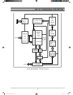
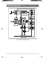
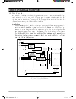
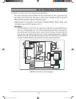
Flash Memory : MX29F040QC-70 (for DVD-DX500 and DVD-DX50)
This stores every program required for the operation of DVD player and holds the data of
OSD languages and LOGO and send them upon request from u-COM. This allows the update
of firmware by CD-R/RW. For DVD module, 8MBit Flash Memory on 52K x 6bit basis is
used.
Description
The MX29F040 is a 4-mega bit Flash memory organizedas 52K bytes of 8 bits. MX-
IC's Flash memories offerthe most cost-effective and reliable read/write non-volatile
random access memory. The MX29F040 is packaged in 32-pin PLCC, TSOP, PDIP. It is
designed to bereprogrammed and erased in system or in standardEPROM programmers.
The standard MX29F040 offers access time as fast as55ns, allowing operation of high-
speed microprocessorswithout wait states. To eliminate bus contention, theMX29F040
has separate chip enable (CE) and outputenable (OE) controls.
MXIC's Flash memories augment EPROM functionalitywith in-circuit electrical erasure
and programming. TheMX29F040 uses a command register to manage thisfunctional-
ity. The command register allows for 00%TTL level control inputs and fixed power
supply levels during erase and programming, while maintaining maxi-mum EPROM
compatibility.
MXIC Flash technology reliably stores memorycontents even after 00,000 erase and
programcycles. The MXIC cell is designed to optimize theerase and program mecha-
nisms. In addition, thecombination of advanced tunnel oxide processingand low in-
ternal electric fields for erase andprogramming operations produces reliable cycling.
The MX29F040 uses a 5.0V±0% VCC supply toperform the High Reliability Erase and
autoProgram/Erase algorithms.
The highest degree of latch-up protection isachieved with MXIC's proprietary non-epi
process.Latch-up protection is proved for stresses up to 00milliamps on address and
data pin from -V to VCC+ V.
Sm(SANYO_DVD-DX500)051220.indd 8
2005-12-29 8:58:41
Содержание DVD-DX500
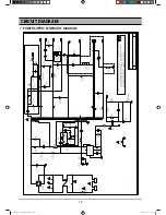
Страница 19: ...18 CIRCUIT DIAGRAM 1 POWER SUPPLY SCHEMATIC DIAGRAM Sm SANYO_DVD DX500 051220 indd 18 2005 12 29 8 58 49 ...
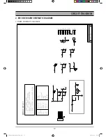
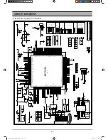
Страница 21: ...CIRCUIT DIAGRAM 20 2 RF MPEG SCHEMATIC DIAGRAM Sm SANYO_DVD DX500 051220 indd 20 2005 12 29 8 58 54 ...
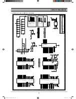
Страница 22: ...CIRCUIT DIAGRAM 21 3 SDRAM FLASH SCHEMATIC DIAGRAM Sm SANYO_DVD DX500 051220 indd 21 2005 12 29 8 58 58 ...
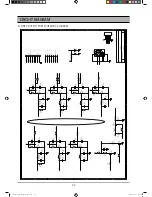
Страница 23: ...CIRCUIT DIAGRAM 22 4 VIDEO OUTPUT PORT SCHEMATIC DIAGRAM Sm SANYO_DVD DX500 051220 indd 22 2005 12 29 8 59 01 ...
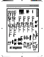
Страница 24: ...CIRCUIT DIAGRAM 23 5 AUDIO OUTPUT PORT SCHEMATIC DIAGRAM Sm SANYO_DVD DX500 051220 indd 23 2005 12 29 8 59 04 ...
Страница 25: ...CIRCUIT DIAGRAM 24 3 CONTROL BOARD SCHEMATIC DIAGRAM Sm SANYO_DVD DX500 051220 indd 24 2005 12 29 8 59 07 ...


