4
CIRCUIT OPERATIONAL DESCRIPTION
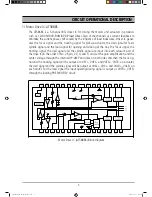
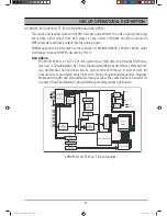
SDROM : PT48046TG-70 (for DVD-DX50)
This sends and receives data with MPEG decoder and performs the video signal processing.
Every video signal output from DVD player is once stored in SDRAM and then encoded in
MPEG decoder and finally output into the analog signal.
SDRAM applied to DVD module has the capacity of 32MBit(048576 x 6bit x 2Bank), sends
and receives data with MPEG decoder by 6 bit.
Description
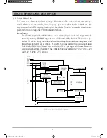
PT48046TG-7 is a high-speed synchronous dynamic random access memory (SDRAM),
organized as M words x 2 banks x 6 bits. Using pipelined architecture and 0.75 m
process technology, PT98646DH delivers a data bandwidth of up to 400M bytes per
second (-5). For different application, PT98646DH is sorted into the following speed
grades: -5, -6, -7. The -5 parts can run up to 200 MHz/CL3. The -6 parts can run up to
66 MHz/CL3. The -7 parts can run up to 43 MHz/CL3. For handheld device applica-
tion, we also provide a low power option, the grade of -7L, with Self Refresh Current
under 400 A and work well at 2.7V during Self Refresh Mode. For special application,
we provide extended temperature option the grade of -6I can work well in wide tem-
perature from -40 C to 85 C.
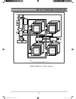
Accesses to the SDRAM are burst oriented. Consecutive memory location in one page
can be accessed at a burst length of , 2, 4, 8 or full page when a bank and row is se-
lected by an ACTIVE command. Column addresses are automatically generated by the
SDRAM internal counter in burst operation. Random column read is also possible by
providing its address at each clock cycle. The multiple bank nature enables interleaving
among internal banks to hide the precharging time.
By having a programmable Mode Register, the system can change burst length, latency
cycle, interleave or sequential burst to maximize its performance. PT98646DH is ideal
for main memory in high performance applications.
Sm(SANYO_DVD-DX500)051220.indd 14
2005-12-29 8:58:45
Содержание DVD-DX500
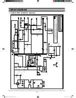
Страница 19: ...18 CIRCUIT DIAGRAM 1 POWER SUPPLY SCHEMATIC DIAGRAM Sm SANYO_DVD DX500 051220 indd 18 2005 12 29 8 58 49 ...
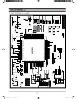
Страница 21: ...CIRCUIT DIAGRAM 20 2 RF MPEG SCHEMATIC DIAGRAM Sm SANYO_DVD DX500 051220 indd 20 2005 12 29 8 58 54 ...
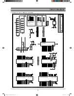
Страница 22: ...CIRCUIT DIAGRAM 21 3 SDRAM FLASH SCHEMATIC DIAGRAM Sm SANYO_DVD DX500 051220 indd 21 2005 12 29 8 58 58 ...
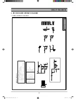
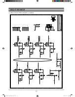
Страница 23: ...CIRCUIT DIAGRAM 22 4 VIDEO OUTPUT PORT SCHEMATIC DIAGRAM Sm SANYO_DVD DX500 051220 indd 22 2005 12 29 8 59 01 ...
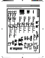
Страница 24: ...CIRCUIT DIAGRAM 23 5 AUDIO OUTPUT PORT SCHEMATIC DIAGRAM Sm SANYO_DVD DX500 051220 indd 23 2005 12 29 8 59 04 ...
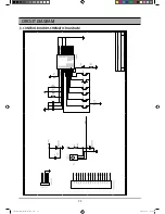
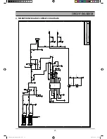
Страница 25: ...CIRCUIT DIAGRAM 24 3 CONTROL BOARD SCHEMATIC DIAGRAM Sm SANYO_DVD DX500 051220 indd 24 2005 12 29 8 59 07 ...


