0
CIRCUIT OPERATIONAL DESCRIPTION
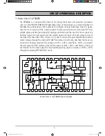
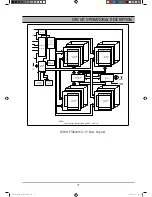
Flash Memory : MX26LV800T/B (for DVD-DX50)
Description
The MX26LV800T/B is a 8-mega bit high speed Flash memory organized as M bytes
of 8 bits or 52K words of 6 bits. MXIC's high speed Flash memories offer the
most cost-effective and reliable read/write non-volatilerandom access memory. The
MX26LV800T/B is pack-aged in 44-pin SOP, 48-pin TSOP, and 48-ball CSP. It is de-
signed to be reprogrammed and erased in system or in standard EPROM programmers.
The standard MX26LV800T/B offers access time as fast as 55ns, allowing operation
of high-speed microprocessors without wait states. To eliminate bus contention, the
MX26LV800T/B has separate chip enable (CE) and output enable (OE) controls.
MXIC's high speed Flash memories augment EPROM functionality with in-circuit electri-
cal erasure and programming. The MX26LV800T/B uses a command register to manage
this functionality. The command register allows for 00% TTL level control inputs and
fixed power supply levels during erase and programming, while main-taining maximum
EPROM compatibility.
MXIC high speed Flash technology reliably stores memory contents even after 00 erase
and program cycles. The MXIC cell is designed to optimize the erase and programming
mechanisms. In addition, the combination of advanced tunnel oxide processing and
low in-ternal electric fields for erase and program operation sproduces reliable cycling.
The MX26LV800T/B uses a3.0V~3.6V VCC supply to perform the High Reliability Erase
and auto Program/Erase algorithms.
The highest degree of latch-up protection is achieved with MXIC's proprietary non-epi
process. Latch-up protection is proved for stresses up to 00 milliamperes on address
and data pin from -V to VCC + V.
Sm(SANYO_DVD-DX500)051220.indd 10
2005-12-29 8:58:42
Содержание DVD-DX500
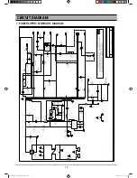
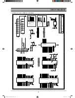
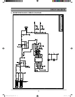
Страница 19: ...18 CIRCUIT DIAGRAM 1 POWER SUPPLY SCHEMATIC DIAGRAM Sm SANYO_DVD DX500 051220 indd 18 2005 12 29 8 58 49 ...
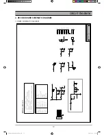
Страница 21: ...CIRCUIT DIAGRAM 20 2 RF MPEG SCHEMATIC DIAGRAM Sm SANYO_DVD DX500 051220 indd 20 2005 12 29 8 58 54 ...
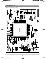
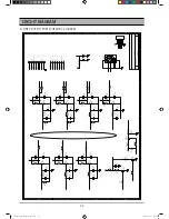
Страница 22: ...CIRCUIT DIAGRAM 21 3 SDRAM FLASH SCHEMATIC DIAGRAM Sm SANYO_DVD DX500 051220 indd 21 2005 12 29 8 58 58 ...
Страница 23: ...CIRCUIT DIAGRAM 22 4 VIDEO OUTPUT PORT SCHEMATIC DIAGRAM Sm SANYO_DVD DX500 051220 indd 22 2005 12 29 8 59 01 ...
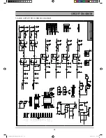
Страница 24: ...CIRCUIT DIAGRAM 23 5 AUDIO OUTPUT PORT SCHEMATIC DIAGRAM Sm SANYO_DVD DX500 051220 indd 23 2005 12 29 8 59 04 ...
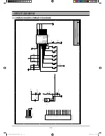
Страница 25: ...CIRCUIT DIAGRAM 24 3 CONTROL BOARD SCHEMATIC DIAGRAM Sm SANYO_DVD DX500 051220 indd 24 2005 12 29 8 59 07 ...


