
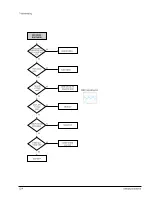


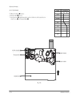


Circuit Operating Description
Samsung Electronics
13-9
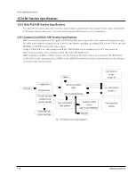
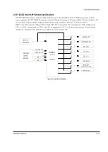
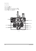
13-3-5 PRML Block H/W Function Specifications
PRML BLOCK performs the data control in each mode using MICOM’s Control Signal. After Head S/W
Pulse is input, it can also consecutively process the signal by separating the high-interval and low-interval
signals of the envelope output during playback.
Receiving the control signal from DV-1 chip, it should be controlled to stop operating (Power Down) during
the REC Time and to process signals normally during the PB Time. Also, it should also be able to perform
playback by providing a 41.85MHz PB Clock and PB Data to the DV-1 chip. Supplied with a 41.85 MHz
signal (or 54 MHz from DSP6) from the DV-1 Chip, it should stably play back by switching the signal to PB
Clock when an unstable signal is received from the PREAMP.
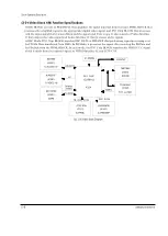
It supplies 41.85 Mbps PB data to the DV-1 Chip after being provided with the playback output signal from
the Differential input (DIP, DIN) of the PREAMP. It also provides a 41.85 MHz PB Clock to the DV-1 Chip by
doubling the 20.925MHz (X2) which is the highest frequency of the playback signal.
It produces an ATF Error Signal from the playback output signal and gives the signal to MICOM Block so
that it can be used as the Capstan Control. It takes two kinds of voltage, 3Vdc and 1.8Vdc from DC/DC and
uses them for internal operating voltage and the reference voltage of this block which is used for controlling
the signal that connects with the exterior. It can also operate the internal 1.8V regulator with an external
option (pull up or pull down). In this case, it can operate at one external operating voltage of 3V.
Содержание VP-D455
Страница 10: ...Product Specification 2 4 Samsung Electronics MEMO...
Страница 30: ...3 20 Alignment and Adjustments Samsung Electronics MEMO...
Страница 46: ...4 16 Disassembly and Reassembly Samsung Electronics MEMO...
Страница 66: ...Exploded View and Parts List 5 20 Samsung Electronics MEMO...
Страница 83: ...Samsung Electronics 8 1 8 Wiring Diagram MEMORY STICK VP D453 I D6620I VP D454 I D455 I D6650I...
Страница 84: ...Wiring Diagram 8 2 Samsung Electronics MEMO...
Страница 86: ...PCB Diagrams 9 2 Samsung Electronics 9 1 Main PCB COMPONENT SIDE...
Страница 87: ...PCB Diagrams Samsung Electronics 9 3 L708 L704 L706 L717 L719...
Страница 88: ...PCB Diagrams 9 4 Samsung Electronics CONDUCTOR SIDE Fuse 1 25A 32V...
Страница 94: ...PCB Diagrams 9 10 Samsung Electronics MEMO...
Страница 114: ...Schematic Diagrams 10 20 Samsung Electronics This Document can not be used without Samsung s authorization MEMO...
Страница 128: ...Troubleshooting 12 8 Samsung Electronics MEMO...
Страница 140: ...Circuit Operating Description 13 12 Samsung Electronics MEMO...
Страница 184: ...Reference Information 14 44 Samsung Electronics MEMO...


