3-35
Samsung Electronics
CIRCUIT DESCRIPTION
Repair Manual
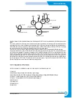
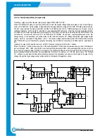
3-5-7-4 MHV (Electrification Output Enable)
Electrification Output Enable is the electrification output control signal 'PWM-LOW ACTIVE'.
When MHV-PWM LOW signal is received, Q401 turns on and the steady voltage will be accepted to the non-inverting ter-
minal of OP-AMP 324. As the voltage higher than the inverting reference voltage of OP-AMP, which is set to R405 and
R406, OP-AMP output turns high. This output sends IB to the TRANS auxiliary wire through current-restricting resis-
tance Q402 via R408 and C403 and Q402 turns on. When the current is accepted to Q402, Ic increases to the current pro-
portional to time through the T401 primary coil, and when it reaches the Hfe limit of Q402, it will not retain the "on" state, but
will turn to "off". As Q402 turns 'off', TRANS N1 will have counter-electromotive force, discharge energy to the sec-
ondary unit, sends current to the load and outputs MHV voltage through the high voltage output enable, which is com-
prised of Regulation– circuit.
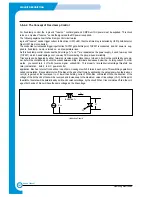
3-5-7-5 BIAS (supply/dev/blade output unit)
BIAS (Electrification Output Enable)Electrification Output Enable is the electrification output control signal ‘PWM-LOW
ACTIVE’.When BIAS-PWM LOW signal is received, Q501 turns on and the steady voltage will be accepted to the non-invert-
ing terminal of OP-AMP 324. As the voltage higher than the inverting reference voltage of OP-AMP, which is set to R506
and R507, OP-AMP output turns high. This output sends IB to the TRANS auxiliary wire through current-restricting
resistance Q502 via R509 and C504 and Q502 turns on. When the current is accepted to Q502, Ic increases to the cur-
rent proportional to time through the T201 primary coil, and when it reaches the Hfe limit of Q502, it will not retain the “on”
state, but will turn to “off”. As Q502 turns ‘off’, TRANS N1 will have counter-electromotive force, discharge energy
to the secondary unit, sends current to the load and outputs DEV voltage through the high voltage output enable, which
is comprised of Regulation-circuit.
MHV-PWM
U103 7407
R412 2.2K
18V
Q401 A708
R403 130K
R402
82K
R411 2K
R404
27K
C407
104
R406
2.2K
R405 220K
24VS
+
_
R408
47K
R409
390
KA324
C403
333
Q402
D526
24VS
T401
C404
3K/471
D402
4KV
C406
3K/471
R416
15M
R413
12M
ZD401
150V
OPC
R417
15M
MHV OUTPUT
BIAS-PWM
CON03-#24
U103-A
7407
2
5V
R520
26K
R519
2.2K
R502
2K
R503
100KF
R506
86.6KF
R508
47K
Q502
D526-Y
D502
4KV
C505
2KV 680
C506
3KV 471
ZD501
100V
ZD501
100V
R512
MGR1/2W 12MF
R514
MGR1/2W 50K
BLADE
SUPPLY
DEV
R515
MGR1/2W 50K
R516
MGR1/2W 50K
R509
47K
R510
430
R507
12KF
U101-B
KA324
R504
56.6KF
C501
104
C502
222
C504
333
R511
1W 3
R501
100
Q501
A708-Y
5
6
7
+
_
U1
C503
104
T201
KAB-007
24VS
1
5
2
4
7
6
Содержание SF-830
Страница 112: ...Exploded Views and Parts List 5 34 Samsung Electronics ...
Страница 116: ......
Страница 163: ...4 2 SCHEMATIC DIAGRAMS Samsung Electronics Repair Manual Main Circuit Diagram 2 17 ...
Страница 164: ...4 3 Samsung Electronics SCHEMATIC DIAGRAMS Repair Manual Main Circuit Diagram 3 17 ...
Страница 165: ...4 4 SCHEMATIC DIAGRAMS Samsung Electronics Repair Manual Main Circuit Diagram 4 17 ...
Страница 166: ...4 5 Samsung Electronics SCHEMATIC DIAGRAMS Repair Manual Main Circuit Diagram 5 17 ...
Страница 167: ...4 6 SCHEMATIC DIAGRAMS Samsung Electronics Repair Manual Main Circuit Diagram 6 17 ...
Страница 168: ...4 7 Samsung Electronics SCHEMATIC DIAGRAMS Repair Manual Main Circuit Diagram 7 17 ...
Страница 169: ...4 8 SCHEMATIC DIAGRAMS Samsung Electronics Repair Manual Main Circuit Diagram 8 17 ...
Страница 170: ...4 9 Samsung Electronics SCHEMATIC DIAGRAMS Repair Manual Main Circuit Diagram 9 17 ...
Страница 171: ...4 10 SCHEMATIC DIAGRAMS Samsung Electronics Repair Manual Main Circuit Diagram 10 17 ...
Страница 172: ...4 11 Samsung Electronics SCHEMATIC DIAGRAMS Repair Manual Main Circuit Diagram 11 17 ...
Страница 173: ...4 12 SCHEMATIC DIAGRAMS Samsung Electronics Repair Manual Main Circuit Diagram 12 17 ...
Страница 174: ...4 13 Samsung Electronics SCHEMATIC DIAGRAMS Repair Manual Main Circuit Diagram 13 17 ...
Страница 175: ...4 14 SCHEMATIC DIAGRAMS Samsung Electronics Repair Manual Main Circuit Diagram 14 17 ...
Страница 176: ...4 15 Samsung Electronics SCHEMATIC DIAGRAMS Repair Manual Main Circuit Diagram 15 17 ...
Страница 177: ...4 16 SCHEMATIC DIAGRAMS Samsung Electronics Repair Manual Main Circuit Diagram 16 17 ...
Страница 178: ...4 17 Samsung Electronics SCHEMATIC DIAGRAMS Repair Manual Main Circuit Diagram 17 17 ...
Страница 180: ...4 19 Samsung Electronics SCHEMATIC DIAGRAMS Repair Manual 4 3 OPE Circuit Diagram D9 ...
Страница 181: ...4 20 SCHEMATIC DIAGRAMS Samsung Electronics Repair Manual 4 4 Scan Circuit Diagram ...
Страница 187: ...4 26 SCHEMATIC DIAGRAMS Samsung Electronics Repair Manual 4 8 PTL Circuit Diagram ...
Страница 188: ...4 27 Samsung Electronics SCHEMATIC DIAGRAMS Repair Manual 4 10 Toner_Rx Circuit Diagram ...
Страница 189: ...4 28 SCHEMATIC DIAGRAMS Samsung Electronics Repair Manual 4 11 Toner_Tx Circuit Diagram ...


