3-33
Samsung Electronics
CIRCUIT DESCRIPTION
Repair Manual
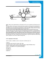
HEAT ROLLER
PRESSURE ROLLER
MHV
LSU
DEV
BLADE
SUPPLY
THV
SUPPLY ROLLER
DEVELOPER ROLLER
DIRECTION OF PAPER
ELECTRIFICATION
ROLLER
TRANSFER ROLLER
direction, it keeps the toner particles between two rollers supplied to OPC drum in negative state by the friction between two
rollers.
The toner supplied to the developer roller is biased to bias electric potential by the developer roller and transferred to the
developing area. After (-) toner is attached to the developer roller, it will move to the exposed high electric potential surface (-
180V) rather than to the unexposed low electric potential surface (-900V) of the developer roller and OPC drum. Eventually
the toner will not settle in the low electric potential surface to form the visible image.
Later, the OPC drum continues to rotate and reaches to transfer location in order to accomplish the transfer process.
This process transfers the (-)toner on the transfer roller to the printing paper by the transfer roller. The (-)toner attached to the
OPC drum will be energized to hundreds to thousands of the (+)transfer voltage by HVPS. The (+)electrostatic force of the
transfer roller generated has higher adhesiveness than the (-)toner OPC drum and thus it moves to the surface of the paper
passing through the transfer roller. The toner transferred to the paper with weak electrostatic force is fixed to the paper by the
pressure and heat of the fixer composed of pressure roller and heat roller. The toner attached to the paper is melted by apply-
ing the heat (approx. 180°C) from the heat roller and the pressure (approx. 4kg) from the pressure roller. After the fixing
process, the paper is sent out of the set to finish the printing process.
3-5-7-3. Organization of the Device
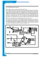
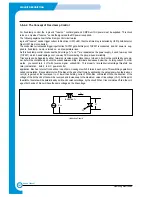
HVPS is comprised of electrification output unit, bias output unit and transfer output unit.
1) Input Unit
2) Electrification Output (Enable) Unit: MHV (Main High Voltage)
3) Bias Output (Enable) Unit: DEV (Development Voltage)/Supply(Supply Voltage)/BLADE(Blade Voltage)
4) Transfer ‘+’ Output (Enable) Unit: THV(+)(Transfer High V))
5) Transfer ‘-’ Output (Enable) Unit: THV(-)(Transfer High Voltage(-))
6) Switching Unit
7) Feedback Unit
8) Regulation Unit
9) Output Unit
Содержание SF-830
Страница 112: ...Exploded Views and Parts List 5 34 Samsung Electronics ...
Страница 116: ......
Страница 163: ...4 2 SCHEMATIC DIAGRAMS Samsung Electronics Repair Manual Main Circuit Diagram 2 17 ...
Страница 164: ...4 3 Samsung Electronics SCHEMATIC DIAGRAMS Repair Manual Main Circuit Diagram 3 17 ...
Страница 165: ...4 4 SCHEMATIC DIAGRAMS Samsung Electronics Repair Manual Main Circuit Diagram 4 17 ...
Страница 166: ...4 5 Samsung Electronics SCHEMATIC DIAGRAMS Repair Manual Main Circuit Diagram 5 17 ...
Страница 167: ...4 6 SCHEMATIC DIAGRAMS Samsung Electronics Repair Manual Main Circuit Diagram 6 17 ...
Страница 168: ...4 7 Samsung Electronics SCHEMATIC DIAGRAMS Repair Manual Main Circuit Diagram 7 17 ...
Страница 169: ...4 8 SCHEMATIC DIAGRAMS Samsung Electronics Repair Manual Main Circuit Diagram 8 17 ...
Страница 170: ...4 9 Samsung Electronics SCHEMATIC DIAGRAMS Repair Manual Main Circuit Diagram 9 17 ...
Страница 171: ...4 10 SCHEMATIC DIAGRAMS Samsung Electronics Repair Manual Main Circuit Diagram 10 17 ...
Страница 172: ...4 11 Samsung Electronics SCHEMATIC DIAGRAMS Repair Manual Main Circuit Diagram 11 17 ...
Страница 173: ...4 12 SCHEMATIC DIAGRAMS Samsung Electronics Repair Manual Main Circuit Diagram 12 17 ...
Страница 174: ...4 13 Samsung Electronics SCHEMATIC DIAGRAMS Repair Manual Main Circuit Diagram 13 17 ...
Страница 175: ...4 14 SCHEMATIC DIAGRAMS Samsung Electronics Repair Manual Main Circuit Diagram 14 17 ...
Страница 176: ...4 15 Samsung Electronics SCHEMATIC DIAGRAMS Repair Manual Main Circuit Diagram 15 17 ...
Страница 177: ...4 16 SCHEMATIC DIAGRAMS Samsung Electronics Repair Manual Main Circuit Diagram 16 17 ...
Страница 178: ...4 17 Samsung Electronics SCHEMATIC DIAGRAMS Repair Manual Main Circuit Diagram 17 17 ...
Страница 180: ...4 19 Samsung Electronics SCHEMATIC DIAGRAMS Repair Manual 4 3 OPE Circuit Diagram D9 ...
Страница 181: ...4 20 SCHEMATIC DIAGRAMS Samsung Electronics Repair Manual 4 4 Scan Circuit Diagram ...
Страница 187: ...4 26 SCHEMATIC DIAGRAMS Samsung Electronics Repair Manual 4 8 PTL Circuit Diagram ...
Страница 188: ...4 27 Samsung Electronics SCHEMATIC DIAGRAMS Repair Manual 4 10 Toner_Rx Circuit Diagram ...
Страница 189: ...4 28 SCHEMATIC DIAGRAMS Samsung Electronics Repair Manual 4 11 Toner_Tx Circuit Diagram ...


