3-37
Samsung Electronics
CIRCUIT DESCRIPTION
Repair Manual
3-5-7-7. Environment Recognition
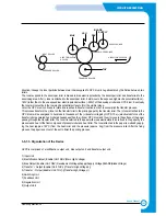
THV voltage recognizes changes in transfer roller environment and allows the voltage suitable for the environment in order
to realize optimum image output. The analog input is converted to digital output by the comparator that recognizes the
environmental changes of the transfer roller. It is to allow the right transfer voltage to perform appropriate environmental
response considering the environment and the type of paper depending on this digital output by the programs that can
be input to the engine controller ROM.
This environment recognition setting is organized as follows: First, set the THV(+) standard voltage.
Allow 200M
Ω
load to transfer output, enable output and set the standard voltage 800V using VR201.
Then set 56 (CPU's recognition index value) as the standard using VR302.
This standard value with CPU makes sure that the current feedback is 4µA when output voltage is 800V and load is 200M
Ω
.
If the load shows different resistance value when 800V is output, the current feedback will also be different and thus the
index value will also be different. according to the index value read by CPU, the transfer voltage output will differ according
to the preset transfer table.
The changes in transfer output required by each load is controlled by PWM-DUTY.
Содержание SF-830
Страница 112: ...Exploded Views and Parts List 5 34 Samsung Electronics ...
Страница 116: ......
Страница 163: ...4 2 SCHEMATIC DIAGRAMS Samsung Electronics Repair Manual Main Circuit Diagram 2 17 ...
Страница 164: ...4 3 Samsung Electronics SCHEMATIC DIAGRAMS Repair Manual Main Circuit Diagram 3 17 ...
Страница 165: ...4 4 SCHEMATIC DIAGRAMS Samsung Electronics Repair Manual Main Circuit Diagram 4 17 ...
Страница 166: ...4 5 Samsung Electronics SCHEMATIC DIAGRAMS Repair Manual Main Circuit Diagram 5 17 ...
Страница 167: ...4 6 SCHEMATIC DIAGRAMS Samsung Electronics Repair Manual Main Circuit Diagram 6 17 ...
Страница 168: ...4 7 Samsung Electronics SCHEMATIC DIAGRAMS Repair Manual Main Circuit Diagram 7 17 ...
Страница 169: ...4 8 SCHEMATIC DIAGRAMS Samsung Electronics Repair Manual Main Circuit Diagram 8 17 ...
Страница 170: ...4 9 Samsung Electronics SCHEMATIC DIAGRAMS Repair Manual Main Circuit Diagram 9 17 ...
Страница 171: ...4 10 SCHEMATIC DIAGRAMS Samsung Electronics Repair Manual Main Circuit Diagram 10 17 ...
Страница 172: ...4 11 Samsung Electronics SCHEMATIC DIAGRAMS Repair Manual Main Circuit Diagram 11 17 ...
Страница 173: ...4 12 SCHEMATIC DIAGRAMS Samsung Electronics Repair Manual Main Circuit Diagram 12 17 ...
Страница 174: ...4 13 Samsung Electronics SCHEMATIC DIAGRAMS Repair Manual Main Circuit Diagram 13 17 ...
Страница 175: ...4 14 SCHEMATIC DIAGRAMS Samsung Electronics Repair Manual Main Circuit Diagram 14 17 ...
Страница 176: ...4 15 Samsung Electronics SCHEMATIC DIAGRAMS Repair Manual Main Circuit Diagram 15 17 ...
Страница 177: ...4 16 SCHEMATIC DIAGRAMS Samsung Electronics Repair Manual Main Circuit Diagram 16 17 ...
Страница 178: ...4 17 Samsung Electronics SCHEMATIC DIAGRAMS Repair Manual Main Circuit Diagram 17 17 ...
Страница 180: ...4 19 Samsung Electronics SCHEMATIC DIAGRAMS Repair Manual 4 3 OPE Circuit Diagram D9 ...
Страница 181: ...4 20 SCHEMATIC DIAGRAMS Samsung Electronics Repair Manual 4 4 Scan Circuit Diagram ...
Страница 187: ...4 26 SCHEMATIC DIAGRAMS Samsung Electronics Repair Manual 4 8 PTL Circuit Diagram ...
Страница 188: ...4 27 Samsung Electronics SCHEMATIC DIAGRAMS Repair Manual 4 10 Toner_Rx Circuit Diagram ...
Страница 189: ...4 28 SCHEMATIC DIAGRAMS Samsung Electronics Repair Manual 4 11 Toner_Tx Circuit Diagram ...

