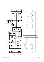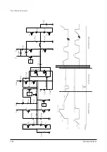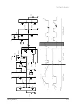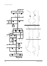
Circuit Operation Description
Samsung Electronics
5-39
(2) Logic main board
!
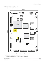
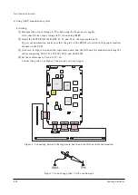
Set the logic main board as Figure 6 shows.
fl
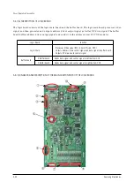
Check for the test PROM installation status and clock jumper setting.
@
Connect a 4-pin connector cable between LD01 of the logic main board and the linear power supply.
(or SMPS).
fl
Connect while the linear power supply (or SMPS) is turned off.
#
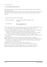
Turn the linear power supply on and supply 5V power to the logic main board.
Check if LED, LD2000 on the left top of the board blinks at about 1 second interval. If the logic board
doesn’t operate normally, the LED will blink too fast or not be lighted on.
$
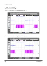
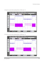
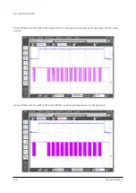
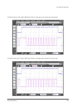
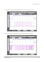
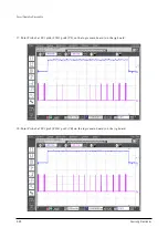
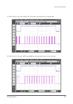
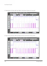
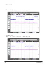
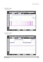
Measure the waveform of each test point on the board, and then compare them with the appended
waveforms.
You should examine the waveforms of all test points.
If the waveform of a test point is different from the appended waveform, or the voltage level is low, do
not proceed to the next examination step and check other abnormal test points.
%
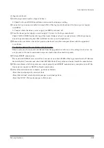
Perform RESET examination.
Press and hold SW2001 reset switch for 5 seconds to turn the LE2000 of the logic main board off. Release
the switch after 5 seconds and check that LD2000 blinks. If no problem is found, finish the examination.
^
If the waveforms of all test points are output properly and RESET examination is complete, turn off the
linear power supply (or SMPS) to finish examination.
&
After all examinations are complete, perform as follows.
- Reset the clock jumper to external clock.
- Reset the internal/external pattern jumper to external pattern.
- Reset the NTSC/PAL mode jumper to PAL mode.
Содержание PPM42S2X/XAA
Страница 2: ...ELECTRONICS Samsung Electronics Co Ltd APR 2002 Printed in Korea AA82 ...
Страница 10: ...3 2 Samsung Electronics MENO ...
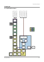
Страница 25: ...Circuit Operation Description Samsung Electronics 5 3 5 1 2 D PDP PS 42 BLOCK DIAGRAM ...
Страница 38: ...Circuit Operation Description 5 16 Samsung Electronics 5 2 3 D DRIVER CIRCUIT DIAGRAM ...
Страница 39: ...Circuit Operation Description Samsung Electronics 5 17 5 2 3 E DRIVER BOARD CONNECTOR LAYOUT ...
Страница 40: ...Circuit Operation Description 5 18 Samsung Electronics ...
Страница 41: ...Circuit Operation Description Samsung Electronics 5 19 ...
Страница 42: ...Circuit Operation Description 5 20 Samsung Electronics ...
Страница 43: ...Circuit Operation Description Samsung Electronics 5 21 ...
Страница 44: ...Circuit Operation Description 5 22 Samsung Electronics ...
Страница 45: ...Circuit Operation Description Samsung Electronics 5 23 ...
Страница 46: ...Circuit Operation Description 5 24 Samsung Electronics ...
Страница 47: ...Circuit Operation Description Samsung Electronics 5 25 ...
Страница 48: ...Circuit Operation Description 5 26 Samsung Electronics ...
Страница 49: ...Circuit Operation Description Samsung Electronics 5 27 ...
Страница 50: ...Circuit Operation Description 5 28 Samsung Electronics ...
Страница 51: ...Circuit Operation Description Samsung Electronics 5 29 ...
Страница 52: ...Circuit Operation Description 5 30 Samsung Electronics ...
Страница 53: ...Circuit Operation Description Samsung Electronics 5 31 5 3 Logic part 5 3 1 Logic Board Block diagram ...
Страница 76: ...Circuit Operation Description 5 54 Samsung Electronics 29 Jig board U1 LE01 pin35 30 Jig board U1 LE01 pin46 ...
Страница 77: ...Circuit Operation Description Samsung Electronics 5 55 31 Jig board U2 LE02 pin35 32 Jig board U2 LE02 pin46 ...
Страница 82: ...Circuit Operation Description 5 60 Samsung Electronics ...
Страница 83: ...Circuit Operation Description Samsung Electronics 5 61 ...
Страница 84: ...Circuit Operation Description 5 62 Samsung Electronics MEMO ...
Страница 93: ...Exploded View Parts List Samsung Electronics 7 1 7 Exploded View Parts List 7 1 PPM42S2X XAA ...
Страница 106: ...Electrical Parts List 8 12 Samsung Electronics MEMO ...
Страница 128: ...10 14 Samsung Electronics MEMO ...
Страница 130: ...11 2 Samsung Electronics MENO ...
Страница 133: ...Samsung Electronics Schematic Diagrams 12 3 TP01 12 3 SCALER3 3D COMB FILTER TP01 CVBS IN ...
Страница 134: ...Schematic Diagrams 12 4 Samsung Electronics 12 4 SCALER4 VIDEO DECODER PIP FIRST IN OUTPUT ...
Страница 135: ...Samsung Electronics Schematic Diagrams 12 5 12 5 SCALER5 VIDEO DA CON ...
Страница 137: ...Samsung Electronics Schematic Diagrams 12 7 12 7 SCALER7 ADC VIDEO TP20 TP21 TP19 TP19 HS OUT TP20 VHS TP21 VCLK ...
Страница 138: ...Schematic Diagrams 12 8 Samsung Electronics 12 8 SCALER8 ADC PC TP23 TP24 TP22 TP22 MHSYNC TP23 MHS TP24 PCLK ...
Страница 140: ...Schematic Diagrams 12 10 Samsung Electronics 12 10 SCALER10 POWER DEGUGER MEMORY REMOCON RS232 RTC ...
Страница 141: ...Samsung Electronics Schematic Diagrams 12 11 12 11 SOUND ...
Страница 143: ...Samsung Electronics Schematic Diagrams 12 13 12 13 CONTROL REMOCON CONTROL REMOCON ...

