


Alignment and Adjustments
2-18
Samsung Electronics
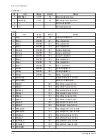
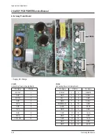
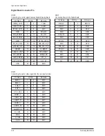
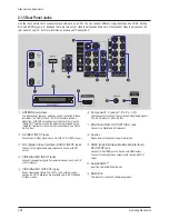
PIN NAME
DESCRIPTION
SCTRL_BN/P
B channel LVDS serial control
DCLK_BN/P
B channel LVDS CLOCK
SCPDI
SERIAL CONTROL DATA INPUT
SCPDO
SERIAL CONTROL DATA OUTPUT
SCPENB
SERIAL CONTROL ENABLE
SCPCK
SERIAL CONTROL CLOCK
DMD RESETB
DMD LOGIC RESET
MBRST(14:0)
MIRROR BIAS RESET
MBRST_EXTRA
UNUSED MIRROR BIAS RESET
SCR_CLR
TEST CLEAR PINS(NORMAL GND)
READOUTA(1:0)
A-CHANNEL SERIAL DATA OUT DURING SPAM READ TEST OPERATION
READOUTB(1:0)
B-CHANNEL SERIAL DATA OUT DURING SPAM READ TEST OPERATION
TP(2:0)
MANUFACTORING TEST POINT(NO CONNECTED DURING NORMAL CPERATION)
RSV_A(4:0)/RSV_B(4:0)
RESERVED PINS(NORMAL:GND)
EVCC
REFERENCE VOLTAGE DURING SPAM READ TEST OPERATION(NORMAL GND)
VCC2
MIRROR ELECTRODE VOLTAGE(7.3V)
VCC
LOGIC SUPPLY
VSS
LOGIC GROUND
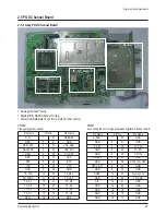
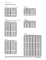
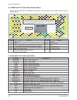
2-9-3 DMD Panel Pin Terminal Characteristics Diagram
2-9-4 Description of Terminal Characteristics
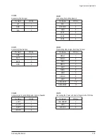
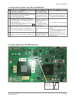
The vertical lines, which may occur due to improper connections between the panel and the
PCB, occur with intervals of 50 inches(26mm). If vertical lines occur with intervals of more than
26mms, it indicates a failure of the DDP1011 IC itself. If they occur with intervals of less than
26mm, it means that more than two pins have bad connections.
DA,DB output wave
[Screen:WHITE]
※
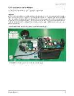
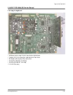
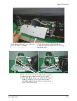
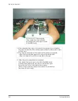
Remove the heat sink attached to the DMD Board and tighten the screws in four places and then inspect the characteristics of
each pin terminal.
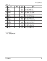
Pin Name
Description
Pin Name
Description
V
Voltage : 3.3V
T
Test Point
V2
VCC2 : 8V
ME
Mirror Bias Extra
DA
A Channel Data Bus [When measured, there should be a waveform]
C
Clock
DB
B Channel Data Bus [When measured, there should be a waveform]
P#
A,B Channel Positive
No.
MBRST# (Mirror Bias Rest) 26V
N#
A,B Channel Negative
G
The part from the present position to the GND
(The black part is also a GND.)
Содержание HL-R5677W - 56" Rear Projection TV
Страница 4: ...1 2 Samsung Electronics MEMO ...
Страница 34: ...2 30 Samsung Electronics MEMO ...


