2 CIRCUIT DESCRIPTION
RT2047 DSC - PART II
When the radio is switched on the dividing figure corresponding to the first figure in the selcall number
is put on port A on the µC which is connected to the input of U18-6. If the correct tone is received the output
of the comparator U15/1-6 goes low. This output is connected to the µC’s INT-pin. When the tone
disappears again the µC will put out the dividing figure corresponding to the next figure in the selcall
number. If all five tones are received correctly then the µC will send a message on the serial interface to
the keyboard unit, turn on the selcall relay RE2-9 (on the filter unit), and send out an alarm tone from PC1
via the volume control and power amp. to the loudspeaker. The alarm tone lasts for 10 seconds after an
individual call and after an all call it lasts until the selcall is reset. If the SELCALL TEST button is activated
the alarm circuits and indicators will be tested.
2.6.13 THE EEPROM
The EEPROM contains an address/opcode register, a data I/O register, a memory array, an internal high
voltage generator (V
pp
) and some decoding logic. The Serial Data Clock (CK) is fed from PC7 on the µC
and all communication starts with the µC setting PC5 thus enabling the Chip Select (CS) on the eeprom
(U8-6). Instructions to U8-6 consists of a dummy 1, a 2 bit opcode, an 8 bit address and for some
instructions also a 16 bit data word. When the opcode is 00 the 2 first bits in the address serve as an
extended opcode.
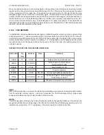
INSTRUCTION SET FOR THE EEPROM (NMC93C56):
,QVWUXFWLRQ
2S
$GGUHVV
'DWD
&RPPHQW
FRGH
READ
10
A7-A0
Reads data at specified address
EWEN
0
11XXXXXX
Write enable, must precede all
programming modes
ERASE
11
A7-A0
Erase register A7-A0
ERAL
0
10XXXXXX
Erase all registers
WRITE
1
A7-A0
D15-D0
Writes reg if address unprotected
WRAL
0
01XXXXXX
D15-D0
Writes all registers. Valid only when
Protect Reg is cleared
EWDS
0
00XXXXXX
Disables all programming instructions
READ:
After a Read instruction is received, the instruction and address are decoded, followed by data transfer
from the selected memory register. A dummy 0 precedes the 16-bit data output string. Output data
changes are initiated by a low to high trasition of the SK clock.
WRITE:
The Write operation is followed by 16 bits of data to be written to the specified address. CS must then be
brought low before the next rising edge of the SK clock to initiate the self-timed programming cycle. D0
indicates the ready state ( 1/0 => ready/busy ) the chip is ready for another instruction.
PAGE 2-20
9543
Содержание RT2047
Страница 1: ...S P RADIO A S AALBORG DENMARK TECHNICAL MANUAL FOR COMPACT VHF RT2047 D ...
Страница 2: ......
Страница 5: ...RT2047 DSC PART I CONTENTS 1 GENERAL INFORMATION 1 1 1 1 INTRODUCTION 1 1 ...
Страница 6: ......
Страница 8: ......
Страница 10: ......
Страница 24: ......
Страница 30: ...1 GENERAL INFORMATION RT2047 DSC PART II PAGE 1 6 9543 ...
Страница 32: ......
Страница 34: ......
Страница 46: ...2 CIRCUIT DESCRIPTION RT2047 DSC PART II PAGE 2 12 9543 ...
Страница 50: ...2 CIRCUIT DESCRIPTION RT2047 DSC PART II 9543 PAGE 2 16 ...
Страница 66: ...9546 ...
Страница 67: ...2 CIRCUIT DESCRIPTION RT2047 DSC PART II 9546 PAGE 2 33 32162 ...
Страница 81: ......
Страница 82: ......
Страница 84: ......
Страница 85: ...PAGE 3 1 9545 3 MECHANICAL DISASSEMBLING AND MODULE LOCATION 3 1 MECHANICAL DISASSEMBLING RT2047 DSC PART II ...
Страница 86: ...3 MECHANICAL DISASSEMBLING AND MODULE LOCATION RT2047 DSC PART II PAGE 3 2 9545 ...
Страница 88: ......
Страница 90: ......
Страница 98: ...4 SERVICE RT2047 DSC PART II PAGE 4 8 9545 ...
Страница 99: ...4 SERVICE RT2047 DSC PART II 4 11 PIN CONFIGURATION 9545 PAGE 4 9 ...
Страница 101: ...4 SERVICE RT2047 DSC PART II NMC93C56N PIN ARRANGEMENT BLOCK DIAGRAM LM393N PIN ARRANGEMENT PAGE 4 11 9545 ...
Страница 109: ...RT2047 DSC PART II CONTENTS 5 PARTS LISTS 5 1 9546 ...
Страница 110: ......
Страница 124: ......

