6. Interlock Switches
•
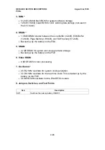
The fusing unit interlock switch (+24V) disables the power supply to the
drive components and the power pack.
•
The fusing unit interlock switch (+5V) disables the laser diode power.
7. Jumpers, Switches, and Test Points
Item
Description
TP1
COM2 ground
TP2
COM1 ground
TP3
+5VE
TP4
-5V
TP7
Laser synchronization signal
TP6
Scanner clock
TP8
Scanner clock
TP9
Analog video signal input from the Contact Image Sensor
CN40-1
Analog video signal
CN40-2
Scanner clock
CN40-3
Synchronization signal
CN40-4
COM1 ground
TB1
Switches the power supply to the flash ROM boot block on the FCE
1-2 pins shorted: +12V (the boot block can be overwritten)
2-3 pins shorted: +5V (the boot block cannot be overwritten)
Warning: Do not change this jumper setting, unless the boot block in
the Flash ROM needs to be overwritten by Function 12.
(Refer to Chapter 4.1.20 for more details.)
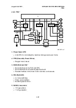
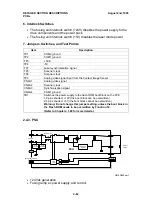
2.4.3. PSU
•
+24Vdc generation
•
Fusing lamp ac power supply and control.
PSU
ACN
ACL
HTN
HTL
F1
Surge
Protection
Surge
Protection
F2
Phase
Control
Switching
Circuit
+24V
COM3
AC Input
Fusing Lamp Output
1HTORON
1HTON
+24VM
GND
Interlock
Switch
Main Switch
H516D532.wmf
DETAILED SECTION DESCRIPTIONS
August 2nd, 1995
PCBs
2-62

