Renesas RA Family
RA2 Quick Design Guide
R01AN6060EU0100 Rev.1.00
Page 22 of 44
Sep.14.21
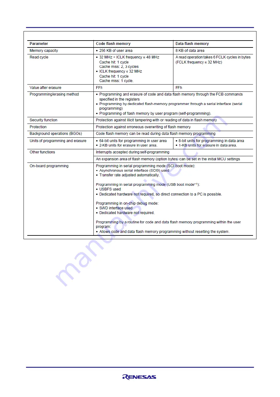
Figure 15. Specifications of Code Flash Memory and Data Flash Memory on RA2A1 MCU
Note:
Erase state of code flash is FFh but erase state of data flash is undefined.
7.3.1 Background Operation
RA2 MCUs support background operations for code flash and data flash. This means that when a program
or erase starts, the user can keep executing and accessing memory from memory areas other than the one
being operated on. For example, the CPU can execute application code from code flash while the data flash
memory is being erased or programmed. Also, the CPU can execute application code from SRAM while the
code flash memory is being erased or programmed. The only exception to this rule is that the data flash
cannot be accessed during code flash programming or erasing.
7.3.2 ID Code Protection
RA2 MCUs have a 128-bit memory in option setting memory area that is used as an ID code. If this ID code
is left blank (0xFF’s) then no protection is enabled and access to the MCU is allowed through boot mode or
using the on-chip debugger. If the ID code is set then the user can control access to these modes. The user
can choose to always disallow connections or can choose to allow connections when a matching ID code is
input. Refer to the “OCD/Serial Programmer ID Setting Register (OSIS)” and “ID Code Protection” and
sections of RA2 MCU Hardware User’s Manual for more information.
Renesas FSP configurator provides options to set up ID code protection for RA2 MCUs as shown in Figure
16.


