5G Module Series
RM505Q-AE Hardware Design
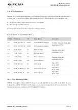
RM505Q-AE_Hardware_Design 24 / 79
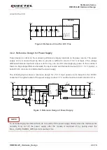
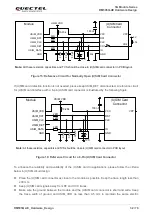
circuit for the VCC.
Module
PMU
2, 4, 70, 72, 74
C1
100
μ
F
D1
5.1 V
3, 5, 11, 27,
33, 39, 45,
51, 57, 71,
73
VCC
VCC
GND
C5
10 pF
C4
33 pF
C3
100 nF
C2
1
μ
F
+
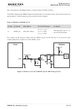
Figure 4: Reference Circuit for VCC Pins
3.4.2. Reference Design for Power Supply
Power design is critical as the
module’s performance largely depends on its power source. The power
supply of the module should be able to provide a sufficient current of 3.0 A at least. If the voltage
difference between input and output is not too big, use an LDO when supplying power to the module. If
there is a big voltage difference between the input source and the desired output (VCC = 3.7 V typical), a
buck DC-DC converter is preferred as the power supply.
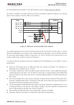
The following figure shows a reference design for +5.0 V input power source based on the DC-DC
converter. The typical output of the power supply is about 3.7 V and the maximum load current is 3.0 A.
D1
TVS
PWR_IN
C8
220 μ
F
C11
10 pF
C10
33 pF
C9
100 nF
+
R1
205k
U1
Q1
NPN
R8
47k
R7
4.7k
PWR_EN
R4
182k
PWR_OUT
L1
1.5
μ
H
VI N
VI N
VI N
EN
VSNS
COMP
RT/CLK
SS
PH
PH
PH
BOOT
PWRGD
GND
GND
AG ND
VFB
R5
330k 1%
R6
100k 1%
C6
100 nF
PWRGD
EP
R2
80.6k
C7
10 nF
R3
10k
C4
10 nF
C5
NM
VFB
C2
100 nF
C3
33 pF
C1
470 μ
F
+
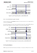
Figure 5: Reference Design of Power Supply
To avoid damaging the internal flash, do not switch off the power supply directly when the module works
normally. Only cut off the power supply after the module is switched off by pulling down the
FULL_CARD_POWER_OFF# pin for more than 10 s.
NOTE


