5G Module Series
RM505Q-AE Hardware Design
RM505Q-AE_Hardware_Design 23 / 79
3.4. Power Supply
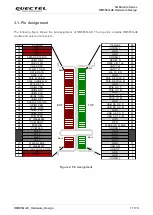
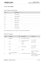
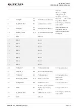
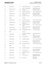
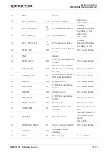
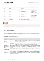
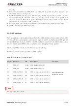
The following table shows pin definition of VCC pins and ground pins.
Table 6: Definition of VCC and GND Pins
3.4.1. Decrease Voltage Drop
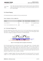
The power supply range of the module is from 3.135 V to 4.4 V. Ensure that the input voltage will never
drop below 3.135 V, otherwise the module will be powered off automatically. The following figure shows
the maximum voltage drop during burst transmission in 3G/4G/5G networks.
VCC
Burst Tr ansmission
Min.3.135 V
Volt age Ripple
< 100 mV
Volt age Drop
Burst Transmission
Figure 3: Power Supply Limits during Radio Transmission
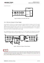
The main power supply from an external system must be a single voltage source. To decrease voltage
drop, an energy storage capacitor of about 100 µF with low ESR (ESR = 0.7
Ω) should be used, and a
multi-layer ceramic chip capacitor (MLCC) array should also be used due to its ultra-low ESR. It is
recommended to use four ceramic capacitors (1 µF, 100 nF, 33 pF, 10 pF) for composing the MLCC array,
and place these capacitors close to VCC pins. The width of VCC trace should be no less than 2.0 mm. In
principle, the longer the VCC trace is, the wider it should be.
In addition, to guarantee stability of the power supply, please use a zener diode with a reverse zener
voltage of 5.1 V and a dissipation power of higher than 0.5 W. The following figure shows a reference
Power Down
Mode
In this mode, the power management unit shuts down the power supply. Software is
inactive, the serial interfaces are inaccessible, and the operating voltage (connected to
VCC) remains applied.
Pin No.
Pin Name
I/O
Power Domain
Description
2, 4, 70, 72, 74
VCC
PI
3.135
–4.4 V
3.7 V typical DC supply
3, 5, 11, 27, 33, 39, 45, 51, 57, 71, 73
GND
Ground

