5G Module Series
RM505Q-AE Hardware Design
RM505Q-AE_Hardware_Design 15 / 79
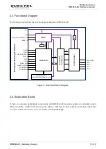
2.3. Functional Diagram
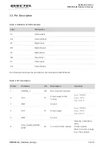
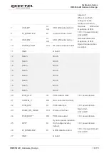
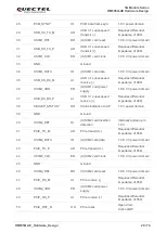
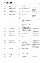
The following figure shows the functional block diagram of RM505Q-AE.
Baseband
PMIC
S
u
b
-6
G
H
z
T
ra
n
s
c
e
iv
e
r
ANT0
ANT3
ANT2
E
T
VCC
RESET_N
38.4M
XO
S
P
M
I
IQ
Control
Tx
PRx
DRx
P
C
I
E
x
p
re
s
s
M
.2
K
e
y
-B
I
n
te
rf
a
c
e
FULL_CARD_POWER_OFF#
W_DISABLE2#
USB 2.0 & USB 3.1
(U)SIM1
WWAN_LED#
WAKE_ON_WAN#
4Gb NAND 4Gb x8
4Gb LPDDR4X SDRAM 4Gb x16
RFFE
W_DISABLE1#
GPIOs
T
x
/R
x
B
lo
c
k
s
ANT1
PCIe
×
1
(U)SIM2
GND
ANT4_GNSS
Figure 1: Functional Block Diagram
2.4. Evaluation Board
To help you develop applications conveniently with RM505Q-AE, Quectel supplies an evaluation board
(PCIe Card EVB), a USB to RS-232 converter cable, a USB type-C cable, antennas and other peripherals
to control or test the module. For more details, see
document [1]
.

