Important
note
Service Manual
PCB Replacement Procedures
7 - 28
3x3 UPS
Issue 2 - November 2001
7.9 - PCB Replacement Procedures
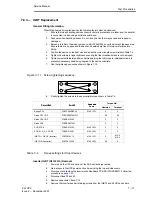
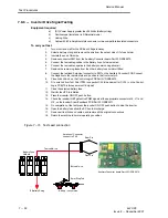
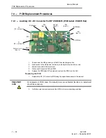
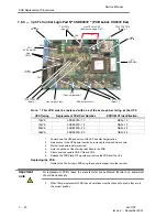
7.9.1 - Auxiliary DC Ć DC Converter Part Nº 0SDE0070 (PCB Label: CS0070 Exx)
PM1
PM2
P1 (500Vdc)
P2 (320Vdc)
P3 (500Vdc)
F2
(DC ćve Input 1A)
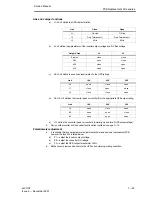
U2A pin1
(See
13.
)
R36
(See
13.
)
R39
(See
13.
)
R37
(See
13.
)
PM2 pin 1 to 6
(See
13.
)
F1
(DC +ve Input 1A)
1.
Power down the UPS and carry out the DC bus discharge routine.
2.
Gain access to the UPS power section by removing the top and side covers.
3.
Mark all connectors before removal.
4.
Disconnect Connector PM1 and PM2.
5.
Release the PCB StandĆOff mounts and remover the PCB from the Unit.
Replacing the PCB
1.
Replace the DC Ć DC converter PCB using the opposite sequence to the removal.
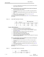
All replacement PCB's leave the manufacturer pre calibrated therefore no adjustment
should be necessary.
2.
Refit all covers removed and return the UPS to its normal operating condition.

