


PMDX-132 User’s Manual
PCB Revision: PCB-466A
Document Revision: 1.0
Serial Numbers: 23410 and above
PMDX-132_Manual_10.doc
©2008 Practical Micro Design, Inc.
Page 9 of 24
17 April 2008
All Rights Reserved
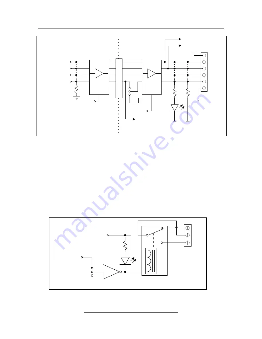
Figure 5 – Block diagram of control signals
3.3
Relay Outputs
Two of the control outputs on the PMDX-132 may drive the on-board relays in addition to being general-
purpose outputs (see section 3.2). PC parallel port pin 1 controls relay K1 via jumper JP3, and pin 14
controls relay K2 via jumper JP4. These two jumpers allow the relays to be disabled when the control
outputs are used as “logic only” outputs. The block diagram below shows the block diagram of one of the
relay circuits. The other circuit is identical but uses the second set of reference designators. See section
5.3 for more information on the jumper settings.
Each relay driver circuit has its own LED (in addition to the LED on the control output section as
described in section 3.2). The relay LED lights when the relay is energized (i.e. the “COM” terminal is
connected to the “N/O” terminal).
Figure 6 – Block diagram of relay output signals
**
Each of the four
signals have their
own LED and
pull-down resistor
Enable
2.2K
2
1
3
JP2
PC Connector
Buffer
(~Strobe) pin 1
(~AutoFeed) pin 14
(~Init) pin 16
(~Selelct In) pin 17
I
S
O
L
A
T
E
Enable
Buffer
+5V
10K
Isolated Pin 17
(to charge pump)
OK (from
charge pump)
To JP3 (relay K1 control)
To JP4 (relay K2 control)
J9
+5V
+5V Aux
pin 1
pin 14
pin 16
pin 17
GND
Equipment Ground
PC Ground
**
**
**
**
**
**
**
**
10K
*
*
*
*
*
Each of the four
input signals have
their own pull-down
resistor
Always
Enabled
2
1
3
N/C
COM
N/O
J3 or J4
K1 or K2
Relay
Driver
Disable
JP3 or JP4
Relay
Power
Relay K1 Control
or
Relay K2 Control
(from Control Signal
block diagram)


