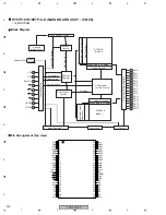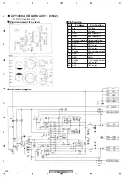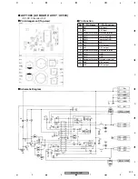
PDP-5050SX
212
1
2
3
4
1
2
3
4
C
D
F
A
B
E
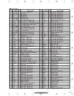
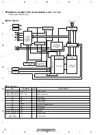
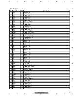
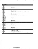
No.
Pin Name
I/O
Pin Function
63
1
8
15
22
30
60
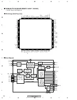
TV
V1
V2
V3
V4
V5
V6
I
Video signal inputs.
Input composite video signals.
3
10
17
24
49
Y1
Y2
Y3
Y4
YIN1
I
Y/C separation signal inputs.
Input luminance signals.
The YIN1 pin inputs the signal obtained by Y/C separating the VOUT1 pin output.
5
12
19
26
51
C1
C2
C3
C4
CIN1
I
Y/C separation signal inputs.
Input chrominance signals.
The CIN1 pin inputs the signal obtained by Y/C separating the VOUT1 pin output.
62, 2
9, 16
23, 29
59, 64
4, 11
18, 25
31, 61
LTV, LV1
LV2, LV3
LV4, LV5
LV6, RTV
RV1, RV2
RV3, RV4
RV5, RV6
I
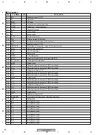
Audio signal inputs.
53
41
VOUT1
VOUT3
O
Video signal outputs.
Output composite video signals.
44
V/YOUT2
O
Video signal output.
Either composite video signal output or luminance signal output can be selected by I2C bus control.
56
YOUT1
O
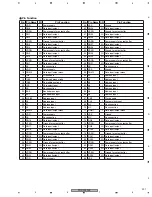
Video signal outputs.
Output luminance signals.
39
YOUT3
58
47
37
COUT1
COUT2
COUT3
O
Video signal outputs.
Output chrominance signals.
52
43
38
54
45
40
LOUT1
LOUT2
LOUT3
ROUT1
ROUT2
ROUT3
O
Audio signal outputs.
Zo=50 ohm (within DC
±
2mA)
6
13
20
27
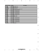
S2-1
S2-2
S2-3
S2-4
−
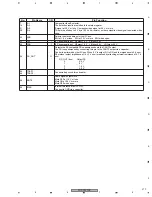
Detects the S2-compatible DC superimposed onto the C signal.
4 : 3 video signal at 1.3 V or less
4 : 3 letter-box signal at 1.3 V or more to 2.5 V or less
16 : 9 picture squeezed signal at 2.5 V or more
This pin is pulled down to GND by a 100 k ohm resistor, so the 4 : 3 video signal is selected when
open.
Pin Function
Содержание PDP4350SX
Страница 9: ...PDP 5050SX 9 5 6 7 8 5 6 7 8 C D F A B E ...
Страница 51: ...PDP 5050SX 51 5 6 7 8 5 6 7 8 C D F A B E ...

