background image

162

PDP-5020FD

1

2

3

4

A

B

C

D

E

F

1

2

3

4

2.  When manual adjustment is required after the DIGITAL Assy is replaced with one 
 for 

service

If backup data cannot be transferred to the DIGITAL Assy because of defective parts, etc., after the DIGITAL Assy is replaced 
and manual adjustment is performed, those manually adjusted data can be registered as adjusted data with the following 
procedures. Once the data on the DIGITAL Assy are registered as adjusted data, the adjustment data for backup will be 
automatically updated each time the unit is turned off. Therefore, if a DIGITAL Assy with adjusted data is mounted on the unit, 
the following procedures are not required, even after manual adjustment.

PANEL INFORMATION

ETC. (+)

BACKUP DATA : NO OPRT

Key Down 7th

Key Down

SET

Right

SET (5 sec)

DIGITAL EEPROM : NO OPRT

DIGITAL EEPROM : REPAIR

(1) Copying, using the Factory menu

1

  Turn on the power.

2

  Enter the Panel Factory mode.

3

  Display the PANEL INFORMATION page, then check if "NO DATA!" is set for "DIG. EEP".

4

  Register the changed adjustment data as adjusted data, as described for the following procedures, then transfer them as 

 backup 

data.

(2) Copying, using the RS-232C commands

1

  Turn on the power.

2

  Issue the FAY command.

3

  With the QS2 command, confirm that the main unit adjustment flag is "adjustment not completed."

4

  Issue the FAJ command to register the changed adjustment data as adjusted data then transfer them as backup data.

5

  With the QS2 command, confirm that the main unit adjustment flag becomes "adjustment completed."

6

  Turn off the power.

5

  Check if "ADJUSTED" is set for "DIG. EEP" on the PANEL INFORMATION page.

6

  Turn off the power.

Содержание ARP3476

Страница 1: ... 9120 Melsele Belgium PIONEER ELECTRONICS ASIACENTRE PTE LTD 253 Alexandra Road 04 01 Singapore 159936 PIONEER CORPORATION 2008 2008 Printed in Japan PDP 5020FD ARP3476 FLAT PANEL TV PDP 5020FD THIS MANUAL IS APPLICABLE TO THE FOLLOWING MODEL S AND TYPE S Model Type Power Requirement Remarks PDP 5020FD KUCXC AC 120 V For details refer to Important Check Points for good servicing T IZS 001 MAY ...

Страница 2: ...be put back in place such as barriers nonmetallic knobs adjustment and compartment covershields isolation resistor capacitor etc 3 When service is required observe the original lead dress Extra precaution should be taken to assure correct lead dress in the high voltage circuitry area 4 Always use the manufacture s replacement components Especially critical components as indicated on the circuit di...

Страница 3: ... not exceed 1 mA ANY MEASUREMENTS NOT WITHIN THE LIMITS OUTLINED ABOVE ARE INDICATIVE OF A POTENTIAL SHOCK HAZARD AND MUST BE CORRECTED BEFORE RETURNING THE SET TO THE CUSTOMER PRODUCT SAFETY NOTICE Many electrical and mechanical parts in PIONEER set have special safety related characteristics These are often not evident from visual inspection nor the protection afforded by them necessarily can be...

Страница 4: ... the product Please check that neither solder debris nor screws remain inside the product 8 There should be no semi broken wires scratches melting etc on the coating of the power cord Damaged power cords may lead to fire accidents so please be sure that there are no damages If you find a damaged power cord please exchange it with a suitable one 9 There should be no spark traces or similar marks on...

Страница 5: ... 5 3 DIAGNOSIS OF PD POWER DOWN 72 5 4 DIAGNOSIS OF SD SHUTDOWN 76 5 5 NON FAILURE INFORMATION 80 5 6 OUTLINE OF THE OPERATION 82 5 7 OUTLINE OF RS 232C COMMAND 87 5 8 LIST OF RS 232C COMMANDS 88 5 9 DETAILS OF EACH COMMANDS 97 6 SERVICE FACTORY MODE 111 6 1 OUTLINE OF THE SERVICE FACTORY MODE 111 6 2 DETAILS OF FACTORY MENU 119 6 3 DIGITAL TUNER SERVICE MENU 144 7 DISASSEMBLY 146 7 1 FLOWCHART OF...

Страница 6: ...ely 40 ºC Therefore for lead free soldering the tip temperature of a soldering iron must be set to around 373 ºC in general although the temperature depends on the heat capacity of the PC board on which reworking is required and the weight of the tip of the soldering iron Do NOT use a soldering iron whose tip temperature cannot be controlled Compared with eutectic solders lead free solders have hi...

Страница 7: ...he current 1 Power Cord 2 AC Inlet 3 Power Switch 4 Fuse In the POWER SUPPLY Unit 5 STB Transformer and Converter Transformer In the POWER SUPPLY Unit 6 Other primary side of the POWER SUPPLY Unit AC inlet Power switch Part is Charged Section Charged Section The places where voltage is 100 V or more except for the charged places described above If the places are touched there is a risk of electric...

Страница 8: ...ol AXD1561 Power cord 2 m 6 6 feet ADG1215 Cable clamps 4 Alkaline dry cell battery LR6 AA 2 Screws to Metal Fittings 2 M4 35 mm Falling Prevention Metal Fittings 2 Cleaning cloth AED1285 Warranty card Operating instructions ARE1488 Fall Prevention Steel Assy AXY1218 Binder Assy AEC2158 ...

Страница 9: ...9 PDP 5020FD 5 6 7 8 5 6 7 8 A B C D E F Speaker accessories Speaker Mounting Screws 9 M5 10 mm SBA1292 Speaker cables 2 SDS1202 Speaker Speaker Bracket Center SXG1159 Speaker Brackets Side 2 SXG1158 ...

Страница 10: ...10 PDP 5020FD 1 2 3 4 A B C D E F 1 2 3 4 2 2 SPECIFICATIONS ...

Страница 11: ...11 PDP 5020FD 5 6 7 8 5 6 7 8 A B C D E F ...

Страница 12: ...12 PDP 5020FD 1 2 3 4 A B C D E F 1 2 3 4 2 3 PANEL FACILITIES Front Section ...

Страница 13: ...13 PDP 5020FD 5 6 7 8 5 6 7 8 A B C D E F Rear Section ...

Страница 14: ...14 PDP 5020FD 1 2 3 4 A B C D E F 1 2 3 4 Remote Control Unit ...

Страница 15: ...15 PDP 5020FD 5 6 7 8 5 6 7 8 A B C D E F ...

Страница 16: ...checked 1 Check if all the symptoms pointed out by the customer have been addressed The symptoms in question must not be reproduced 2 Connect the peripheral equipment Connect all external peripheral equipment as originally connected and check if the connections are correct 3 Check the video and audio Tune in to the stations that the customer would normally receive and check if video and audio are ...

Страница 17: ... ENTER SET press j seven times press ENTER SET then press j six times 2 Press l to select CLEAR Hold ENTER SET pressed for at least 5 seconds After clearance is completed ETC is automatically selected Clear the maximum temperature value MAX TEMP in the same manner 4 Other Assys Clearance of the maximum temperature value 1 Select PANEL FACTORY ETC then MAX TEMP After entering Factory mode press MUT...

Страница 18: ...T 5 CTI 6 CC To shift to another mode press MUTING To shift to another item in a specific mode press i or j To shift to the next nested layer below for an item with a indication press ENTER SET To return to the next nested layer above also press ENTER SET Mode transition in Service Factory mode Up Down Structure of Layers in Panel Factory Mode 2 8 ETC 1 BACKUP DATA 2 DIGITAL EEPROM 3 PD INFO 4 SD ...

Страница 19: ...0 50F DIGITAL Assy AWW1347 50F X DRIVE ASSY AWV2546 50F Y DRIVE ASSY AWV2547 Mark No Description Part No MAIN ASSY AWW1371 SIDE HDMI ASSY AWW1372 IO_AUDIO ASSY AWW1352 SIDE IO ASSY AWW1356 PC ASSY AWW1359 SIDE KEY ASSY AWW1361 LED ASSY AWW1362 IR ASSY AWW1363 FAN CONNECT ASSY AWW1364 RLS ASSY AWW1365 POWER SW ASSY AWW1366 POWER SUPPLY UNIT AXY1200 PDP SERVICE ASSY 509F AWU1339 Note The wiring show...

Страница 20: ...20 PDP 5020FD 1 2 3 4 A B C D E F 1 2 3 4 3 4 JIGS LIST Service Cotton Cloth Glove GYX1002 7 3 DISASSEMBLY AND REASSEMBLY PRECAUTIONS FOR SPEAKER SYSTEM Name Jig No Remarks ...

Страница 21: ...21 PDP 5020FD 5 6 7 8 5 6 7 8 A B C D E F ...

Страница 22: ...22 PDP 5020FD 1 2 3 4 A B C D E F 1 2 3 4 4 BLOCK DIAGRAM 4 1 OVERALL WIRING DIAGRAM 1 2 ...

Страница 23: ...D k When ordering service parts be sure to refer to EXPLODED VIEWS and PARTS LIST or PCB PARTS LIST k The mark found on some component parts indicates the importance of the safety factor of the part Therefore when replacing be sure to use parts of identical designation ...

Страница 24: ...24 PDP 5020FD 1 2 3 4 A B C D E F 1 2 3 4 4 2 OVERALL WIRING DIAGRAM 2 2 F0015 FERRITE CORE ATX1069 F0016 FERRITE CORE ATX1069 ...

Страница 25: ...25 PDP 5020FD 5 6 7 8 5 6 7 8 A B C D E F OVERALL DIAGRAM PDP 5020FD ...

Страница 26: ... B VDDLS1 VDDLS2 VDDLS3 VDDLS4 RESONANCE BLOCK RESONANCE BLOCK RESONANCE BLOCK RESONANCE BLOCK AN P BN P CN P DN P CLKN P ADDRESS L ASSY AD2 CN1601 IC1601 LVDS RECEIVER AD1 CN1602 VADR1 VADR2 VADR3 VADR4 V 10V V 75V V 3 3V CLK LE HBLK LBLK R G B VDDLS1 VDDLS2 VDDLS3 VDDLS4 RESONANCE BLOCK RESONANCE BLOCK RESONANCE BLOCK RESONANCE BLOCK AN P BN P CN P DN P CLKN P ADDRESS L ASSY AD2 CN1601 IC1601 LV...

Страница 27: ...NANCE BLOCK RESONANCE BLOCK AD1 CN1602 VADR1 VADR1 VADR2 VADR2 VADR3 VADR3 VADR4 V 75V V 10V V 10V V 3 3V V 75V V 3 3V CLK LE HBLK LBLK R G B CLK LE HBLK LBLK R G B VDDLS1 VDDLS1 VDDLS2 VDDLS2 VDDLS3 VDDLS3 VDDLS4 RESONANCE BLOCK IC1801 LVDS RECEIVER RESONANCE BLOCK RESONANCE BLOCK RESONANCE BLOCK RESONANCE BLOCK RESONANCE BLOCK RESONANCE BLOCK AN P BN P CN P DN P CLKN P AN P BN P CN P DN P CLKN P...

Страница 28: ...Digital Audio signal Component signal Synchronized signal RF signal Control signal Data signal IC4701 HY57V641620FTP 64Mbit SDRAM Add0 12 Data0 15 CLP CN8802 PC Input CVBS Y C CVBS JA7881 SPDIF INPUT4 HDMI INPUT5 HDMI INPUT6 HDMI CLP CVBS L R IN L R IN OPT_OUT Input2 Y CB CR PB PR JA8551 SPEAKER TERMINAL IC5501 MN884350 DS_IF_P DS_IF_N IC6001 BCM7404 LAN IC6403 AGC1082 S29GL25N90TFIRI 256Mbit FLAS...

Страница 29: ...078 S29GL016A90TFIR2 16Mbit Flash IR KEY1 KEY2 KEY REM LED SR_OUT TXD_SR RXD_SR TXD_232C RXD_232C DIN1_DVO 12bit IC7004 BR24L64F EEPROM IC7201 EDD5116AFTA 512Mbit DDR IC7202 AGC1073 S29GL032A90TFIR4 32Mbit FLASH Add0 12 Data0 15 FAN DIN2 8Bit 3 INT H V EXT H V M11 CN4209 M10 CN4201 M5 CN4202 RLS M15 CN4208 RLS RGB 10bit 3 RGB 10bit 3 FAN FAN FAN Fan Connect IC7302 CXB1443R HDMI SW H2 JA7302 M20 JA...

Страница 30: ... RELAY EXT_PD T702 T501 P3 P2 P1 P6 P5 6 5V VSUS_ADJ Q704 Q703 Switching Switching P4 P10 17V 17V 6 5V 17V 12V F102 B for RELAY DRIVE DRF_SW_B M_SW_DET PD_TRIG_B DRF_B Q902 Q901 Q503 Q502 Switching Switching 12V STB5 1V 17V 6 5V VADR VSUS D101 395V P9 Switching 12V 6 5V 17V D108 T101 P7 Switching IC101 STB3 4V D112 Q202 AC_DET M_SW_DET IC202 6 5V D115 AC_DET ...

Страница 31: ...31 PDP 5020FD 5 6 7 8 5 6 7 8 A B C D E F ...

Страница 32: ...XKOFS1 VXKOFS2 VSUS SUS BLOCK Gate Signal Gate Signal Gate Signal Drive Signal RESONANCE BLOCK PSUS 5V OFFSET Reg Drive Signal SUS PreDrive VPU 17V VSUS SUS BLOCK VSUS SUS BLOCK SOFT D XPRST VSUS 17V PSUS LOGIC BLOCK 17V 15V DC DC CONV VPU VPOFS 17V 5V VSUS 6 5V X 2 REG X 3 VADR VADR VADR X 4 50F X DRIVE ASSY ...

Страница 33: ... IC5V VH IC5V VH IC5V VH IC5V VH IC5V VH IC5V VH IC5V VH IC5V VH IC5V SCAN SIGNAL VH VH IC5V IC5V Y 1 PSUS PSUS Scan Signal IC5V Y 5 17V IC5V VF DC DC CONV IC5V VC_P 17V 15V DC DC CONV VC_S VC_U 5V Drive Signal VSUS VYPRST VSNOFS VKNOFS2 VKNOFS3 VKNOFS4 VKNOFS1 MAIN DC DC CONV VH Y 2 Photo Coupler BLOCK VSUS SUS BLOCK VSUS SUS BLOCK VSUS SUS BLOCK SUS PreDrive 17V VC_S H MSK VC_S L MSK 17V KNOFS1 ...

Страница 34: ... XPRST FET XSOFT D FET XKOFS1 FET Pre drive XKOFS2 FET Pre drive XKOFS1 Reg XKOFS2 Reg Logic SUS G IGBT Pre drive SUS B IGBT Pre drive SUS U IGBT Pre drive SUS D IGBT Pre drive LMSK FET Pre drive YPRST FET Pre drive SNOFS FET Pre drive YKOFS 1 FET Pre drive YKOFS 2 FET Pre drive YKOFS 3 FET Pre drive YKOFS 4 FET Pre drive RST D FET Pre drive VYKOFS 12 Reg VYKOFS 3 Reg VYKOFS 4 Reg DC DC Conv VSNOF...

Страница 35: ...Y VADR1 VADR1 VADR2 VADR2 VADR3 VADR3 VADR4 V 75V V 10V V 10V V 3 3V V 75V V 3 3V CLK LE HBLK LBLK R G B CLK LE HBLK LBLK R G B VDDLS1 VDDLS1 VDDLS2 VDDLS2 VDDLS3 VDDLS3 VDDLS4 RESONANCE BLOCK IC1801 LVDS RECEIVER RESONANCE BLOCK RESONANCE BLOCK RESONANCE BLOCK RESONANCE BLOCK RESONANCE BLOCK RESONANCE BLOCK AN P BN P CN P DN P CLKN P AN P BN P CN P DN P CLKN P AD2 CN1801 AD1 CN1802 AD2 CN1601 AD1...

Страница 36: ...T_SQ V 3V_D EXT_PD RST2 SUS_MUTE EVI_R G B EVI_SYNC DRF_B KDD D14 D15 D16 D22 D18 D19 D20 D17 RESETX AND V 1_1V_D V 2_5V_D V 2_5V_D V 1_2V_D V 2_5V_D V 1_8V_D D26 V 3_3V_D 10V REG 1 2V REG 1 8V REG V 12V V 10V UART CS YSUS DET_CS D12 WE_SQ RELAY1 SUS_MUTE AND AND GPIO8 PSW2 V 3_3V_D V 10V V 3_3V_D V 10V V 3_3V_D V 10V V 3_3V_D V 10V V 3_3V_D V 10V V 3_3V_D V 10V V 3_3V_D V 10V V 3_3V_D V 10V RELAY...

Страница 37: ... DECODER LA72702NVA A E TBB IC5301 SIF MODE_SEL 7404_I2C1_SCL 7404_I2C1_SDA DVO 12bit TS0 EBI BUS MEMORY BUS RXD_DT TXD_DT From EMMA2 To ARIA From To EMMA2 To MAP AGC IF SW IC5303 SCL_AV SDA_AV From USB Connector CN4107 FLASH 256M IC6403 I2S DS_IF_P DS_IF_N 1Chip System IC BCM7404XKPB11G K IC6001 From LAN Connector JA6001 IF_AGC AIR_L AIR R To AV SW I2C_TUNER_SCL I2C_TUNER_SDA I2C SW IC5304 DIGITA...

Страница 38: ...8V A V 3_3V_A2 3 3V 1 5 2 V 3_3V_A2_VDEC V 31_5V_ANT 30V 3 V 31_5V_ANT TUNER SW REG CONTROLED BY RELAY IC4302 Variable REG FAN_VCC1 PQ200WNA1ZPH IC4303 Variable REG FAN_VCC2 PQ200WNA1ZPH IC4305 5V REG V 5V_ANT NJM2846DL3_05 IC4308 DD converter V 31_5V_ANT IC 3V REG V 3V_A FAN_CONT2 FAN_CONT2 V 2_6V_D V 5_1V_D V 5V_D IC4402 DD converter BD8606 Q4412 FET SW V 2_6V_D2 RSS100N03 PSW1_1 V 6_5V V 1_2V_D...

Страница 39: ...V_D4_HDMI V 3_4V_D3_ARIA V 1_8V_D2 1 8V 1 5 V 1_8V_D2_HDMI V 3_4V_D3_ARIA_ROM V 1_8V_D3 1 8V 2 V 1_8V_D3_VDEC V 3_4V_D2 3 4V 3 V 3_4V_D2_BCM V 3_3V_ANT_BCM V 3_4V_D2_FE Q4501 FET SW V 3_4V_ACT RSS090P03 ACTIVE Q4509 FET SW V 3_4V_ACT2 RTQ040P02 V 1_5V_ACT IC4501 DD converter LTC3407 STBY SW REG Q4510 FET SW V 3_4V_D RTQ040P02 V 2_6V_D Q4506 FET SW V 3_4V_D3 RSS090P03 PSW1_1 Q4522 FET SW V 3_3V_D4 ...

Страница 40: ...DCA DC DETECT BLOCK R_OUT L_OUT 17V LPF L OUT R OUT A_NG_B OTW 17V 12V SPDIF_HDMI SPDIF_DTV I2S_BCLK_DTV I2S_LRCLK_DTV I2S_SDATA_DTV RST_MSP SDA_AV SCL_AV SIDE_L R SR_OUT JA7871 SR_OUT TEMPERATURE AC_AM_MUTE AIR_L AIR_R AC_HP_MUTE AC_A_MUTE INPUT1 INPUT2 INPUT4 HDMI L R INPUT5 HDMI L R PC AUDIO OPTICAL OUT SUB WOOFER OUT AUDIO OUT IO_AUDIO ASS Y L_OUT R_OUT SP TERMINAL REGULATOR IC7961 NJM78M12DL1...

Страница 41: ...P_PLUG WP_EDID SDA SCL_AV5 SDA SCL_AV5 SDA SCL_AV5 SIDE_V EMMA_DA_GY EMMA_DA_GY BCB RCR EXT_HD VD INT_HD VD CLP_RGB2 MAIN_C Y SUB_C Y A_TUNER_V RCR BCB GY_AD TEMP2 CN7504 5V 5V IO6 IO5 for MAIN ASSY CN7503 REGULATOR IC7951 NJM2846DL3 18 REGULATOR IC7901 NJM2846DL3 05 REGULATOR IC7911 P0200WNA1ZPH for SIDE ASSY for PC ASSY AV SW IC8001 R2S11006FT RGB SW IC8101 R2S11001FT for MAIN ASSY ...

Страница 42: ...Y POWER SUPPLY UNIT LED ASSY SIDE KEY ASSY MAIN ASSY IO_AUDIO ASSY SIDE IO ASSY PC ASSY IR ASSY RLS ASSY FAN CONNECT ASSY M12 M13 M14 M4 M1 M2 M3 M5 M6 M11 M15 FAN P8 P9 SW1 L1 RL1 RE1 FAN FA1 FA2 FA3 IO5 S1 IO6 IO2 IO3 IO4 IO1 D12 D11 P5 M20 H1 SIDE HDMI ASSY PC1 FAN FAN USB ...

Страница 43: ...of times 2 Notify upon the shutdown content by Blue LED flashing number of times 3 Notify upon the subcategory number by Orange LED flashing number of times 4 Notify upon the abnormal state by Orange LED flashing number of times POWER ON STANDBY SLEEP LED Pattern Remarks Blue Red Orange Blue Red Orange Blue Red Orange Blue Red Orange Blue Red Orange Blue Red Orange Blue Red Orange Blue Red Orange ...

Страница 44: ... to the MOD microcomputer 4 The relay is controlled with logical OR interpretation of control signals by the main microcomputer and module MOD microcomputer MOD Microcomputer IC3601 MAIN Microcomputer IC7003 IF Microcomputer IC6811 Power MOD RELAY Control OR REM Inv Amp Q8751 REM infrared receiver Side Keys SR OUT Jack JA7871 4 1 2 1 RELAY2 SR_OUT KEY_1 KEY_2 TXD_MD RXD_MD REQ_MD SR_IN TXD_IF RXD_...

Страница 45: ...R PS_PD EXT_PD A TUNER D TUNER PD PD PD SW EEPROM DCDC REG D COLOR S AMP DCDC REG DCDC REG ucom TEMP2 RGB SW VDEC HDMI ASIC PS_PD PD_TRG_B EXT_PD RELAY REG AV SW DCDC REG RLS EEPROM SW V 6_5V A D TUNER COFDEM BCM A D TUNER COFDEM CIF BCM HD MSP A D TUNER MPX DEMOD BCM MAP Microcomputer output port setting Microcomputer input port state All devices are not electrified Only the periphery of the IF m...

Страница 46: ...C REG DCDC REG ucom TEMP2 RGB SW VDEC HDMI ASIC PS_PD PD_TRG_B EXT_PD RELAY REG AV SW DCDC REG RLS EEPROM SW V 6_5V A D TUNER COFDEM BCM A D TUNER COFDEM CIF BCM HD MSP A D TUNER MPX DEMOD BCM MAP Microcomputer output port setting Microcomputer input port state Periphery of the IF Main and Module microcomputers are operated The user operation is invalid due to Main Switch off Only the periphery of...

Страница 47: ...D PD_TRG_B EXT_PD RELAY REG AV SW DCDC REG RLS EEPROM SW V 6_5V A D TUNER COFDEM BCM A D TUNER COFDEM CIF BCM HD MSP A D TUNER MPX DEMOD BCM MAP Microcomputer output port setting Microcomputer input port state Periphery of the IF Main and Module microcomputers are operated The user operation is valid AC ON Main Power ON Active Standby AC ON Main Power ON Function Standby OFF ON ON ON ON OFF OFF OF...

Страница 48: ...CDC REG D AMP DCDC REG DCDC REG ucom TEMP2 RGB SW VDEC HDMI ASIC PS_PD PD_TRG_B EXT_PD RELAY AV SW DCDC REG RLS EEPROM SW V 6_5V A D TUNER COFDEM BCM A D TUNER COFDEM CIF BCM HD MSP A D TUNER MPX DEMOD BCM MAP AC Microcomputer output port setting Microcomputer input port state All devices are operated AC ON Main Power ON PDP Screen ON ON ON ON ON ON ON ON ON IF ACTIVE Main RELAY2 Main PSW1 Module ...

Страница 49: ...Y port of the connectors between the DIGITAL Assy and POWER SUPPLY Unit H 3 4 V No No Is the drive off Turn the drive on No Yes Yes Yes A shutdown occurs See 5 4 DIAGNOSIS OF SD SHUTDOWN Yes A power down occurs Does the screen display reset lighting 1 See 5 3 DIAGNOSIS OF PD POWER DOWN Yes When the panel drive power is in OFF state there will be no PD except PS_PD When the panel drive power is in ...

Страница 50: ...y menu Is an external video signal displayed properly Specific failure whose cause is difficult to identify in the initial stage No No Failure analysis for the audio system AU1 Yes Yes Yes In the subsequent diagnostic steps it is most likely that the multi base section is in failure Problems concerning video display Problems concerning the audio output A Failure analysis for the DIGITAL Assy DG1 F...

Страница 51: ...e within the specified range Is there a fluctuation in the VADR voltage Is there a fluctuation in the VSUS voltage The ripple must be within 5 V The ripple must be within 10 V The specified voltage values are between 72 and 78 V The specified voltage values are between 200 and 210 V VSU 125 35 C No Yes Yes No No Yes Yes The cells of the panel do not light normally No The POWER SUPPLY Unit is norma...

Страница 52: ... connectors properly connected to the X Y DRIVE Assys Is the input signal normal Replace the panel chassis Yes Replace the X Y DRIVE Assys NG Replace the DIGITAL Assy Properly connect the panel FPC and SCAN Assys connectors Properly connect the FFC cables No Replace the FFC cables Reset lighting is not displayed Is the waveform normal when the voltage is applied to the panel Failure analysis for t...

Страница 53: ...e oscilloscope photos No Is the waveform of the control signal from the SCAN Assy normal See the oscilloscope photos Failure analysis for the drive system DR2 Because it is difficult to identify which drive is in failure follow the flowchart below to check each Assy Using ADJ1 on the Panel Factory menu or the QAJ command check if the adjustment value is within the range described in the table belo...

Страница 54: ...ll the connectors properly connected Reconnect the connectors B D Yes X DRIVE Assy No Are all the connectors properly connected Reconnect the connectors No C No Yes Is the TCP control signal normal See the oscilloscope photos Yes ADDRESS Assy Replace the panel chassis Replace the DIGITAL Assy Yes No NG Replace the FFC cables Is the input signal normal See the oscilloscope photos Compare the measur...

Страница 55: ...1 CN1302 CN2404 1 CN2401 1 CN2405 1 CN2403 1 CN2406 1 CN1302 1 CN1301 1 Lower side of R2723 3 Upper side of R2621 3 Left side of R2754 3 Right side of R2757 3 Right side of R2755 3 K1402 1 K1401 1 VOFS_ADJ 13 91 55 54 VYPRST_ADJ 62 495 75 2 YVKNOFS1_ADJ 36 85 159 3 YVKNOFS3_ADJ 36 85 159 3 YVKNOFS4_ADJ 36 85 159 3 XKNOFS1_ADJ 27 3 30 XKNOFS2_ADJ 25 0 69 8 VOF value 0 18 9 6 VRP value 0 81 74 4 V1F...

Страница 56: ...e waveform normal when the voltage is applied to the panel See the oscilloscope photos Note1 Note 1 In a case where confirmation of the waveform for a particular line is impossible with an oscilloscope it is possible to identify a defective line by lighting a particular line using the following commands The SCAN IC outputting each line refers to the table PON FAY MKRS01 BSMS01 Command for reducing...

Страница 57: ...from the output of IC2801 on the MAIN Assy to IC3301 on the DIGITAL Assy If only the OSD is abnormal the MAIN Assy is in failure If no vertical sync signal is input to the DIGITAL Assy a freeze frame picture will be displayed It is most likely that the video signal and sync signal data are abnormal No No No NG Failure in connectors CN3201 or CN3202 on the DIGITAL Assy Failure in ASIC IC3301 on the...

Страница 58: ...resetting of the IF microcomputer canceled Failure in the line between the IF microcomputer and M11 connector No Replace the MAIN Assy Yes Is the voltage at Pin 3 of the M11 connector High Relay control is unable unless it supplies a power supply to the module microcompute No Replace the MAIN Assy Yes Is the voltage at Pin 50 of the M4 connector 3 4 V No Replace the MAIN Assy Yes Are the voltages ...

Страница 59: ... the MAIN Assy No Replace the MAIN Assy The input signal is not displayed ATV Is the selected input signal a composite signal Yes No COMP S1 COMP PC2 Is the selected input signal a component signal Yes COMP PC1 Is the selected input signal a S video signal Is the selected input signal an PC signal Yes No Is the selected input signal an HDMI signal Yes Yes DTV 1 Is the selected input signal a digit...

Страница 60: ...e U5301 TUNER Is a signal input to TP7558 No Check the 40P FFC J214 between the MAIN Assy and IO Assy If there was problem replace it Yes Which signal is not output main or sub signal Is a signal output from IC8001 AVSW pin 45 Are the data output from IC4702 VDEC pins 93 to 97 99 to 104 107 to 109 Yes Has the signal arrived at IC4702 VDEC pin 22 Yes Yes Yes Is the communication between each IC VDE...

Страница 61: ...s MAIN SUB 7 6 9 11 Is a signal output from IC8001 pins 47 49 13 12 15 14 8 10 6 IC8001 pin 68 Y V 500 mV div H 20 μsec div 7 IC8001 pin 70 C V 500 mV div H 20 μsec div 8 IC8001 pin 45 Main Y V 500 mV div H 20 μsec div 9 10 IC8001 pin 42 Main C V 500 mV div H 20 μsec div IC4702 pin 22 Main Y V 500 mV div H 20 μsec div 11 IC4702 pin 26 Main C V 500 mV div H 20 μsec div 12 IC8001 pin 49 Sub Y V 500 ...

Страница 62: ...tween IC8101 and microcomuputer If there was no ploblem replace the IO Assy Check the 40P FFC J214 between MAIN Assy and IO Assy If there was problem replace it Check around the IC that is found to have failure in communication and the microcomputer If there was no ploblem replace the MAIN Assy No Replace the MAIN Assy Yes Is the communication between each IC ADC ASIC on the MAIN Assy and the micr...

Страница 63: ...re was problem replace it Check the 12P FFC J215 between IO Assy and PC If there was problem replace it Check around the IC that is found to have failure in communication and the microcomputer If there was no ploblem replace the MAIN Assy No Replace the MAIN Assy Yes Is the communication between each IC ADC ASIC on the MAIN Assy and the microcomputer normal 25 IC8101 pin 2 G in V 500 mV div H 10 μ...

Страница 64: ... LAN or other ambient electromagnetic waves When the dressing of the RF cable is modified does the C N value fluctuate When the RF cable is shortened as much as possible is the symptom cleared No Checking of the reception environment Does the input level become high when the antenna is reoriented Is the signal loss large because multiple distributors are used When a booster or attenuator is added ...

Страница 65: ...y be low If noise is generated with VSB8 multiple paths may be the cause FEC LOCK Check the status of the demodulation IC Check if LOCK is indicated Even if block noise is generated LOCK is indicated if a picture is displayed IF AGC Check the IF AGC voltage Is the IF AGC voltage level high enough The following table provides an indication of the level QAM256 QAM64 VSB8 less than 50 less than 55 le...

Страница 66: ...e in conformity with the specifi cations for this unit No No Reformat the USB memory device Defective USB device Defective USB cable No Replace the USB cable Defective power supply circuit for USB VBUS The data cannot be played back To the check items for DTV Yes dependant Yes Limit of this unit s specifications Is the USB device name displayed on the Factory screen Yes No Replace the MAIN Assy No...

Страница 67: ... Replace the MAIN Assy No Are the properties of the files displayed on the Factory screen Replace the MAIN Assy HMG How to enter DTB Service menu Note Use the remote control unit that supports Factory mode because the DTB Service menu is accessible from Factory mode Step 1 Press the Factory key on the remote control unit to display the INFORMATION screen of Factory mode Step 2 Press the Mute key o...

Страница 68: ...ilure points Is a 12 V output from 12V_Reg output of IC7961 normal Yes Check the peripheral circuits and the communication with the microcomputer If there was no ploblem replace the MAP5601M Are signals input to IC8331 pins 2 3 5 6 Yes Check the IC8331 and peripheral circuit Repair the failure points Are signals output from IC8331 pins 1 7 No Check between the LPF L8451 L8452 and speaker terminals...

Страница 69: ... pins 1 7 Yes Replace the cables or SIDE IO Assy NG Check the cables between CN7505 and CN8601 or check around the Headphones jack B 36 37 41 42 Waveforms Input signal L R 1 kHz 0 5 Vrms VOL 30 38 43 39 44 40 45 46 47 JA8551 pins 1 2 V 2 V div H 1 mS div IC8201 pins 54 55 V 2 V div H 5 μS div JA8551 pins 3 4 V 2 V div H 1 mS div IC8201 pins 24 25 V 2 V div H 1 mS div 46 47 IC8201 pins 38 39 V 1 V ...

Страница 70: ...input to IC8201 pins 100 to 102 Yes Is a SPDIF signal input to IC8201 pin 4 Check the communications around the IC8201 and between the IC8201 and the microcomputer If there was no ploblem replace the MAIN Assy Is a signal output from IC6001 of the MAIN Assy No Repare the DTB block Check around IC6001 and repair the failure points Check between input terminal and IC8201 and repair the failure point...

Страница 71: ...71 PDP 5020FD 5 6 7 8 5 6 7 8 A B C D E F ...

Страница 72: ...connection detection lower VKOFS1_2 VKOFS3 VKOFS4 IC5V VH VPRST Resonance center electric potential Resonance center electric potential Y1 D22 D21 X1 D13 to D20 AD1 OR OR OR DCDC Convertor Stop PD detecdtion Under voltage detection Under voltage detection Under voltage detection Under voltage detection Under voltage detection Under voltage detection Over or under voltage detection Over or under vo...

Страница 73: ...he number of times the Red LED flashes when power down occurs in the corresponding route ADR_PD_MSK ADR_PD DIGI_DCDC_PD XDD_PD XSUS_PD DRF_SW EXT_PD SCN5V_PD SCAN_PD YDD_PD YSUS_PD PS_PD PD_TRG_B PD_MUTE_B DRF_SW P4 D23 MODULE Microcomputer OR OR ADRS_PD Gen PD MUTE circuit DCDC Convertor SQ_LSI Relay Control Protection Circuit ...

Страница 74: ...KNOFS2 block VYKOFS1 2 regulaotr Y MSK block VYKOFS3 regulaotr Y MSK block KNOFS4 block VYKOFS4 regulaotr Over or under voltage protection of the center electric potential Over or under voltage protection of the center electric potential Y resonance block DIGITAL Assy SQ_LSI does not operate SEQ_LSI Sync input output waveform Address resonance block TCP Connector AD1 AD2 DIGITAL Assy Connector D13...

Страница 75: ...602 Q2418 PR U is short circuited Q2662 R2669 L2301 R2335 Q2427 SOFT G is short circuited Q2321 Q2326 Q2328 Q2331 Q2333 Q2334 L MSK is short circuited Q2430 KNOFS2 is short circuited Q2702 Q2705 R2714 Q2321 Q2326 Q2328 Q2331 Q2333 Q2334 L MSK is short circuited Q2703 Q2706 R2715 Q2321 Q2326 Q2328 Q2331 Q2333 Q2334 L MSK is short circuited Q2432 KNOFS4 is short circuited Q2704 Q2707 R2717 Q2106 Q21...

Страница 76: ...3 EMMA2_UCOM TXD_MD RXD_MD A_NG_B RST4 RST2 IC8401 D Amp I04 IC4702 VDEC SCL_AV SDA_AV SCL_AV5 SDA_AV5 SCL_MA SDA_MA IC4801 ADC IC4901 HDMI_RX IC7004 EEPROM IC8001 AV SW IC8101 RGB SW SCL_MB SDA_MB IC6811 IF_UCOM TXD_IF RXD_IF CLK_IF BUSY_IF CE_IF REQ_IF OTW ANT_POW_DE IC5301 MPX U5301 AD FE IC5501 MN884350 IC6001 BCM7404 TXD_DT RXD_DT FAN NG2 M5 2 1 SW 5V 3 3V Converter 1 BLOCK DIAGRAM OF THE SHU...

Страница 77: ...V 6_5V IC6501 MULTI_LSI M12 V 12V V 6_5V V 5_1V IC7002 AND Gate IC7002 AND Gate V 3_4V_ACT2 V 3_4V_D V 3_3V_D3 D11 IC3601 MODULE_UCOM MDU IC3301 SQ_LSI IC3607 MONO MULTI TXD_SQ RXD_SQ CLK_SQ CE_SQ BUSY_SQ RST_SQ IC3805 3 3V_RST_IC IC3602 DIG EEPROM IC3901 SENSOR IC3902 BACKUP EEPROM IC3605 DAC RST2 SQ_NON TEMP1 DAC_DIN DAC_DOUT DAC_CLK E_SCL E_SDA D24 SE1 STOP_SQ FU3801 5A_FUSE IC3801 DDC PLANT R3...

Страница 78: ... DIGITAL memory Digital EEPROM Backup EEPROM DAC IC Abnormality in high temperature Abnormality in low temperature IF microcomputer MULTI Tuner 1 MSP MAP AV switch RGB switch Main VDEC VDEC SDRAM AD PLL HDMI US MSP FAN2 DTV startup error DTV communication error DEVICE ERR Tuner 1 Application DEMOD DC DC Converter power decrease POWER SUPPLY Main EEPROM communication error SQ LSI MD DEV RST2 TMP NG...

Страница 79: ...N4004 IC6001 IC6001 IC6001 IC6001 U5301 IC6001 IC6001 IC5501 IC7002 IC7002 POWER SUPPLY Unit CN4207 CN4210 IC7004 IC7003 SQ_IC communication not established IC3301 may not have properly started up A shutdown occurs if the drive waveform periodically does not output When SQ_NON of MDU input is High a shutdown is generated If BUSY_SQ remains high a shutdown is generated When the identification resis...

Страница 80: ... not possible The video signal output from the DIGITAL connector is copy protected Miscellaneous The no signal off function is not activated The no signal off and no operation off functions are effective only if video composite S video component HDMI excluding PC input or TV input is selected The no operation off function is not activated Power management does not function Power Management is effe...

Страница 81: ...tivation of the protection function return to normal 2000 700 Fig 1 Relationship between input APL and number of SUS pulses Input APL Limiting for the maximum number of SUS pulses Offsetting of the ABL adjustment value The number of SUS pulses with regard to the input APL will be decreased Fig 3 Detection example Protection against panel cracking Fig 2 Detection example SCAN IC protection Protecti...

Страница 82: ...e DRV S00 by RS 232C command DRV S01 for release Supplemental explanation When the panel drive power is in OFF state there will be no PD except PS_PD as the PD signal has been muted If the clip is removed in the OFF state of the panel drive power PD will take place at the instance of clip removal Therefore be sure to remove the clip after turning the power OFF Under RS 232C command control DRV S01...

Страница 83: ...ure of the fan is higher than the ambient temperature because the sensor temperature is read by the microcomputer If the critical values for signals are displayed in the address circuit the fan may be activated or be rotated at higher speed in response to values lower than the set temperature values shown above When the temperature rises the sensor voltage of TEMP2 decreases When the voltage of th...

Страница 84: ...A_NG_B A_NG_B MAIN_UCOM PULL_D OTW OTW MAIN Assy IO_AUDIO Assy 1 Establish the short circuit of the speaker by the main CPU After a warning indication is displayed for 5 sec a shutdown is generated the blue LED flashes 5 times A warning indication is displayed for all input signal types Example of a warning indication The speaker terminals are short circuited After reconnection turn the unit on ag...

Страница 85: ... port outputs are set as specified If the signal at the RST3 port continues to be H after 30 mS of waiting monitoring is continued If RST3 is L a restoration process starts according to the latest power on off status RST4 MAIN power RELAY Shutdown occurs if the signal is L for 5 sec after RELAY2 is ON or for 2 sec while the unit is ON or in Functional STB RELAY2 ON High Shutdown occurs immediately...

Страница 86: ...FAN_NG2 FAN Shutdown occurs when the signal is H 1 S 3 times RST2 H and FAN_ON2 H Monitoring starts 3 sec after the above conditions are established Shutdown occurs immediately Blue LED flashes 10 times RST4 H Monitoring starts 1 sec after the above conditions are established In the Panel screen ON Shutdown occurs after the warning indication is displayed for 30 sec In the Functional STB Shutdown ...

Страница 87: ...like the case of previous models which required switching of exclusive operation between these connectors on the Integrator menu switching is no longer required It is necessary to prepare the following one to use 232C command PC Application for control 232C cable straight The setting of the Com port cannot be communicated if it doesn t do correctly Please follow a set explanation of PC in the Com ...

Страница 88: ...1 CTP Color temperature switch OFF Color temperature switch LOW setting S01 S00 CHN Changing tuner preset channel 1 step forward Changing tuner preset channel 1 step reverse REV FWD Panel drive power OFF S00 Dither L dither OFF noise OFF S01 Dither L dither ON noise ON S02 Dither L dither OFF noise ON S03 Dither L dither ON noise OFF S01 Panel drive power ON A MDU B C D MTB AMT Audio mute OFF AP0 ...

Страница 89: ...rive permission S00 S01 S21 S03 S04 S05 S06 S07 Input switch INPUT 8 PC S08 S01 S02 S03 MIR Mirror display mode OFF Mirror display mode Right and left inversion Mirror display mode Top and bottom inversion Mirror display mode Top and bottom and right and left inversion S00 S01 S02 S03 S04 S05 Erasing afterimage 1 S07 Erasing afterimage 2 S08 White change in luminance level S09 PEAK detection raste...

Страница 90: ... 1 S30 S31 S32 S33 S34 S35 S36 S37 S38 S39 RGB checker 2 Window GREEN GREEN 1023 Even line horizontal stripes Window BLUE BLUE 1023 Window RED RED 1023 Afterimage check 2 Afterimage check 4 MOD S40 Red single color slanting ramp MOD S41 GREEN single color slanting ramp MOD S42 BLUE single color slanting ramp MOD S43 For panel light check 1 MOD S44 For panel light check 2 MOD S45 5 for perfect line...

Страница 91: ...D MOD MOD Raster Green S04 S03 Raster Blue S05 Raster Black S06 Raster Cyan S07 Raster Magenta S08 Raster Yellow S09 Raster Pink MST Display one screen S01 S00 PsideP Main size normal MSE Product form one body monitor model S01 S00 Product form System model S02 PinP Right down S03 PinP Right up S04 PinP Left down S05 PinP Left up S08 SWAP Exchanging sub screen S10 Raster Yellow egg color S11 Raste...

Страница 92: ...For general purpose Japan standard Energy saving 1 S12 For general purpose Japan standard Energy saving 2 PCS S00 Normal operation S01 Catalog specification operation MOD MOD PBX Panel Bx measuring value MOD PBY Panel By measuring value MOD MOD Command Name Function Effective only in Factory mode Active U com Last Memory Remarks MDU MTB P S01 Blue gamma setting Fixed on 1 6 S02 Blue gamma setting ...

Страница 93: ...tion of MTB MR side Acquiring logs of power down points Acquiring data of the pulse meter Acquiring panel white balance adjustment values QPW Acquiring characteristic function setting values of the panel side QPF QS1 Acquiring unit data such as the software version Acquiring data on the status of the unit such as temperature QS2 Q S01 Red gamma setting Fixed on 1 6 S02 Red gamma setting Fixed on 1...

Страница 94: ...econd reset wedge width R1K MOD MOD Command Name Function Effective only in Factory mode Active U com Last Memory Remarks MDU MTB S00 S01 S01 08 Shutdown enabled SDM SFR Shutdown prohibited Measures against AM radio noise Pattern 1 to 8 S MOD SAT Timing adjustment between the scan and address MOD S00 S01 S02 SCW Normal operation Draw the warning blue window left side Draw the warning red window ri...

Страница 95: ...eference value of Vyknofs 1 2 voltage MOD V3F Adjustment of the reference value of Vyknofs 3 voltage MOD V4F Adjustment of the reference value of Vyknofs 4 voltage MOD MOD Adjustment of the reference value of Vysnofs voltage VOF VOL UP DW To adjust the volume Note 4 UAJ Determining the flag for the DIGITAL Assy adjustment in not adjusted UP SZM To add to the adjustment value 0 to 9 add 10 with UP0...

Страница 96: ...il resonance down width 2SF second YSUS resonance up width 2SF repeat YSUS resonance up width Y1Z Y2B MOD 2SF YSUS Tail wedge width Y2K MOD 2SF YSUS Tail resonance down width Y2Z MOD 3SF and later SSF 2 pulses YSUS Tail wedge width YNK MOD 3SF and later YSUS Tail wedge width YTK MOD 3SF and later YSUS Tail resonance down width YTZ YSB ZME Initializing the video EEPROM data of the MTB MR side Z ...

Страница 97: ... 1 byte 19 MTB product form 1 byte 20 Program version of IF microcomputer 8 byte 21 Boot version of IF microcomputer 4 byte 22 Program version of Main microcomputer 8 byte Boot version of Main microcomputer 4 byte 23 Common version of ASIC 8 byte 24 Boot version of ASIC 8 byte 25 PRS version of ASIC 8 byte PIC version of ASIC 8 byte 0A 01A 26 27 Common version of the Digital Tuner 8 byte Boot vers...

Страница 98: ...ted 3 Adjustment data backup flag 0 Adjustment completed 1 Adjustment not completed 4 5 PD data 0 No PD data 2 POWER 3 SCAN 4 SCN 5V 6 Y DCDC 7 Y SUS 8 ADRS A X DCDC 10 1 SD subcategory SQ_LSI 0 No SD Sub data 1 Communication error 2 Drive stop 3 BUSY 4 Version mismatching H S B X SUS C DIG DCDC F UNKNOWN 9 SD data 0 No SD 1 SQ_LSI 2 MDU DEVICE 3 RST2 4 Panel temperature 11 Operation status induce...

Страница 99: ...8 DATA 2 CS 63 Byte 3 QS3 OTHER DATA ON THE PANEL The command QS3 is for acquiring data on operational information of the panel Note 1 Centigrade scale Data Arrangement Data Length Output Example ECO 3 byte QS5 1 Color sensor data Note 1 byte 2 2 RED data of color sensor 4 byte 0425 3 GREEN data of color sensor 4 byte 2112 4 BLUE data of color sensor 4 byte 5000 5 Reserved 32 byte to CS 2 Byte 2 b...

Страница 100: ...SQ_LSI PRG 4 byte 01Y 4 SQ_LSI PIC_TBL 8 byte 01Y 5 SQ_LSI SEQ_DATA 4 byte 01Y 6 CS Reserved 8 byte 2 Byte 2 byte A3 Command Format Effective Operation Modes Function Remarks QSP Every Time Output of status Return data 3 ECO 40 DATA 2 CS 45 Byte 5 QSP SUB VERSION OF THE PANEL SECTION The command QSP is for acquiring sub version data on software of the panel ...

Страница 101: ...128 10 Reserved 6 byte 14 Y1Z adjustment value 3 byte 128 15 X1B adjustment value 3 byte 128 16 Y2B adjustment value 3 byte 128 17 X3B adjustment value 3 byte 128 18 YSB adjustment value 3 byte 128 19 XSB adjustment value 3 byte 128 20 YTK adjustment value 3 byte 128 24 YNK adjustment value 3 byte 128 25 SAT adjustment value 3 byte 128 26 Reserved 3 byte 21 YTZ adjustment value 3 byte 128 22 Y2K a...

Страница 102: ...F 2 ON interlocked with APL 1 ON 11 12 13 RGB Gamma setting n 00 to 31 18 Transition ofprotective operations 0 Upper limit state for brightness 1 Brightness being reduced 2 Lower limit state for brightness 3 Brightness being increased 17 Interlocked with APL 0 OFF 1 ON 2 WB interlocked ON γ OFF 3 WB interlocked OFF γ ON 1 Type of Drive sequence 60VS Video 60 Hz 50VS Video 50 Hz 72VS Video 72 Hz 75...

Страница 103: ... 13 7 ADDRESS U1 U2 setting value 2 byte 32 11 Full screen black display mode 1 byte 1 12 Reserved 4 byte 13 PANEL RX 3 byte 512 8 ADDRESS U3 U4 setting value 2 byte 30 9 Reserved 4 byte 10 Streaking correction 1 byte 1 14 PANEL RY 3 byte 512 15 PANEL GX 3 byte 512 16 PANEL GY 3 byte 512 17 PANEL BX 3 byte 512 18 PANEL BY 3 byte 512 19 Reserved 6 byte 20 Color sensor R coefficient 3 byte 21 Color ...

Страница 104: ...st PD data 1 byte 4 14 Fifth latest 2nd PD data 1 byte 0 15 Data from the hour meter for the fifth latest PD 8 byte 00000715 16 Sixth latest 1st PD data 1 byte A 17 Sixth latest 2nd PD data 1 byte 2 18 Data from the hour meter for the sixth latest PD 8 byte 00000552 19 Seventh latest 1st PD data 1 byte A 20 Seventh latest 2nd PD data 1 byte 0 21 Data from the hour meter for the seventh latest PD 8...

Страница 105: ...t SD data 1 byte 2 17 Sixth latest SD subcategory data 1 byte 2 18 Data from the hour meter for the sixth latest SD 8 byte 00000451 19 Seventh latest SD data 1 byte 0 20 Seventh latest SD subcategory data 1 byte 0 21 Data from the hour meter for the seventh latest SD 8 byte 00000000 22 Eighth latest SD data 1 byte 0 23 Eighth latest SD subcategory data 1 byte 0 24 CS Data from the hour meter for t...

Страница 106: ... 0 STOP 1 LOW 2 HIGH 1 byte 3 A D value of room light sensor 3 byte 4 Level of room light sensor Value 1 to 5 1 byte Command Format Effective Operation Modes Function Remarks QSE Every time Output of status Induce it peculiar individual information is acquired 12 QSE DESTINATION PECULIAR INFORMATION 13 QMT STATUS INFORMATION OF MTB MR SECTION Return data 3 ECO 28 DATA 2 CS 33 Byte Return data 3 EC...

Страница 107: ... byte 7 18 Fifth latest SD subcategory data 1 byte 2 19 Data from the MTB hour meter for the fifth latest SD 7 byte 0105628 20 Reserved 3 byte 000 fixed 21 Sixth latest SD data 1 byte B 22 Sixth latest SD subcategory data 1 byte 0 23 Data from the MTB hour meter for the sixth latest SD 7 byte 0003009 24 CS Reserved 3 byte 000 fixed 25 Seventh latest SD data 1 byte C 26 Seventh latest SD subcategor...

Страница 108: ...ediately Shutdown 6 VDEC SDRAM Immediately Shutdown 7 AD PLL Immediately Shutdown 8 HDMI Immediately Shutdown 9 DisplayPortTx Immediately Shutdown B US MAP Immediately Shutdown C GCR Immediately Shutdown D COFDEM Immediately Shutdown No 7 Subcategory Information on Failure in 3 wire serial communication of Main microcomputer Value Shutdown Factor Remarks Operation 1 Communication error of IF micro...

Страница 109: ... protection operations 1 Byte 0 22 Address emergency status 1 Byte 1 23 CS Detection status of reset operation 1 Byte 1 24 In phase SUS mode status 1 Byte 1 25 Reserved 1 Byte 1 2 Byte 2 Byte 27 Command Format Effective Operation Modes Function Remarks QSI Every Time Output of status Return data 3 ECO 66 DATA 2 CS 71 Byte The command QSI is for acquiring all data on input video signals 18 to 20 Ea...

Страница 110: ... However if the status of the EEPROM on the DIGITAL Assy is adjustment completed the data in the EEPROM of the DIGITAL Assy will be copied to the EEPROM for backup upon POF BCP To copy the backup data from the EEPROM for backup to the EEPROM on the DIGITAL Assy When the DIGITAL Assy is to be replaced adjustment values can be copied from the backup EEPROM to the EEPROM of the Assy for service 17 FA...

Страница 111: ...ANSITION CHART 2 HOW TO ENTER EXIT SERVICE FACTORY MODE By using a PDP service remote control PDP service remote control Press FACTORY key By issuing RS 232C commands During normal Standby mode Issue PON then FAY During normal operation mode Issue FAY By using a PDP service remote control PDP service remote control press FACTORY key Supplied remote control unit press HOME MENU key By issuing RS 23...

Страница 112: ...d in memory will be retained Screen size will be retained The settings for the following functions are set to OFF when Service Factory mode is entered including when the FAY command is received Note Enter the factory after cancelling ACI because the ACI operation setting OFF and not done Fuctions whose setting are set to OFF Function Remarks 2 Screen Operation Input function set on the main side i...

Страница 113: ... 7 etc CH P Increasing the channel number CH P Decreasing the channel number Numeric Keys Function TV Function TV previously selected channel number is selected POWER Power OFF Turning the power off FACTORY Factory OFF Factory mode In Factory mode turning Factory mode off Factory ON Non Factory mode In Non Factory mode turn Fuctory mode on HOME MENU Menu ON In Factory mode turn Factory mode off VO...

Страница 114: ... set the switch to 2 INTEGRATOR Press this key to enter Integrator mode INPUT Press this key to cyclically change the input source EXT INPUT Press this key to cyclically change only the external input source SUB INPUT Not used with this model DRIVE OFF Press this key to turn off the panel drive For details on how to cancel this command see the explanation for the DRV command FACTORY Press this key...

Страница 115: ...KSB 112 to 144 YSTL_1SF_HZ 112 to 144 XSUS_1ST_B 112 to 144 YSUS_2ND_B 112 to 144 XSUS_3RD_B 112 to 144 YSUS_B 112 to 144 XSUS_B 112 to 144 YSTL_KSB 112 to 144 YSTL_HZ 112 to 144 YSTL_2SF_KSB 112 to 144 YSTL_2SF_HZ 112 to 144 YSTL_FMR_KSB 112 to 144 SCAN ADRS ADJ 112 to 144 SUS FREQ MODE 1 to MODE 8 2 6 PANEL 2 ADJ R HIGH 000 to 999 G HIGH 000 to 999 B HIGH 000 to 999 R LOW 000 to 999 G LOW 000 to...

Страница 116: ...V 75V1 75V2 RST MASK 25 2 10 PATTERN MASK SETUP MASK OFF PTN MASK 01 PTN MASK 49 2 11 COMBI MASK SETUP MASK OFF CMB MASK 01 CMB MASK 17 Exclusively used for production line 6 2 4 INITIALIZE for the technical analysis for the technical analysis 1 for the technical analysis 6 2 3 OPTION 3 1 CH PRESET 3 2 ANTENNA MODE 3 3 AFT for the technical analysis 3 4 SYNC DET 3 5 CTI for the technical analysis ...

Страница 117: ...1 1 0 6 0 N T V H A B 20 25 30 35 40 Main item indications Main items Subtitled items Note See SIG Mode Tables See next page 1 Input function 2 SIG mode and Screen size 3 Color system and Signal type Input Functions OSD VIDEO 1 to 7 VD 1 to 7 Terrestrial Wave Analog AIR Cable Analog CBL Terrestrial Wave Digital ARD 4 Option Destination Panel Generation etc Options OSD ELITE PRO 151 111FD AHB Regul...

Страница 118: ... Fv Vertical Frequency Fh Horizontal Frequency 1st to 4th Character Signal Type Fv Hz Fh kHz 10 60 SDTV 525i 60 000 15 750 20 60 SDTV 525p 60 000 31 500 30 60 HDTV 1125i 60 000 33 750 40 60 HDTV 750p 60 000 45 000 50 24 HDTV 1125p 24 000 27 000 50 60 HDTV 1125p 60 000 67 500 k supported unsupported 5th Character GUI Notation VIDEO PC 0 DOT k 1 4 3 k k 2 FULL k k 3 ZOOM k 4 CINEMA k 5 WIDE k 9 WIDE...

Страница 119: ...Item Display Item Meaning Meaning Display Example Program Display Example Boot I F I F microcomputer 07A 01A MAIN Main microcomputer 02KF_1 01K MULTI AGC AGC data of Multi processor 1078 A 01A MULTI PRS Program of Multi processor 02A MULTI PIC Picture quality data of Multi processor 02A DTUNER Software program of the Digital tuner 02K 01K MODULE Module microcomputer 06A 01A SEQ PRS PANEL INFO Prog...

Страница 120: ... V R S I N 2 O T D B A H R D 3 0 4 2 A P S S O W R D 2 1 3 4 A M T I O V D 1 1 1 0 6 0 N T V H A B 1 5 10 15 16 1 5 10 15 20 25 30 35 40 1 2 VERSION 2 Display Item Meaning Display Example DTB HARD DTB Hardware Version 0342 PASSWORD User setting password 1234 ...

Страница 121: ... circuit of the speaker terminal or failure signal of audio amplifier MAIN OTW Short circuit of the speaker terminal or failure signal of audio amplifier IF MA IIC IIC Communication error of Main microcomputer FE1 Tuner 1 MSPMAP MSP MAP AV SW AV Switch RGB SW RGB Switch VDEC Main VDEC SDRAM VDEC SDRAM ADC AD PLL HDMI HDMI US MAP US MAP RETRY Communication error with DTB DEVICE DTB device error DE ...

Страница 122: ...ven if k key or l key is pressed CLEAR YES CLEAR NO is repeated Selecting NO then pressing the ENTER SET key will return the screen to the next higher layer without doing anything Selecting YES then holding the ENTER SET key pressed for 5 seconds will clear the NG log data that are managed in MTB then return the screen to the next higher layer Clear the MAIN NG history ...

Страница 123: ...re conversion display is done with 10 bit the A D input value of IF microcomputer It is displayed by both the Fahrenheit F and 8 bit A D value Note When temperature F of the sensor becomes more than a specified temperature the shutdown start of processing FAN1 The value of the FAN rotating state is displayed STOP stopped LOW slow speed HIGH high speed FAN2 The value of the rotation state of FAN is...

Страница 124: ...R of the panel PANEL 00151H 21M Accumulation power ON count of the panel P COUNT 00000095 TIMES ABCDEFGHIJKLMNO Serial number of the product SERIAL MTB HOUR METER N N I F O R T C M L E A R N O B H R U O M E R T E 8 A M T I O V D 1 1 1 0 6 0 N T V H A B 1 5 10 15 16 1 5 10 15 20 25 30 35 40 Operation Even if k key or l key is pressed CLEAR YES CLEAR NO is repeated Selecting NO then pressing the ENT...

Страница 125: ... R G B Q R E b 2 1 P I X D E P i t 1 5 10 15 16 1 5 10 15 20 25 30 35 40 D I G H A B Displays the input signal information of HDMI terminal Display Item Meaning PWR5V 5 V power detection 18 pin of HDMI terminal VSYNC VSYNC detection CKDT Clock detection SCDT SYNC detection DCRPT HDCP decryption status AUTHEN HDCP authentication status MODE HDMI mode status BIST HDCP Key status Always display it wi...

Страница 126: ...of horizontal pixels V RES Number of vertical lines H DE Number of effectively horizontal pixels V DE Number of effectively vertical lines INTRL Interlace INT or progressive PRG V POL VSYNC polarity H POL HSYNC polarity AUDIO first line Sampling frequency ex DVD 48kHz CD 44 1kHz 1 AUDIO second line Audio format PCM PCM or No PCM no PCM AUDIO third line Quantization bit COL SP Color space AVI Info ...

Страница 127: ...olor system distinction result 096h ACC coefficient 098h 3D YC flag 1B5h MV detection 1 1B6h MV detection 2 1B7h MV detection 3 Sub Address Sub screen 400h 401h 494h 495h 496h 5B5h 5B6h 5B7h 1 8 VDEC SIGNAL INFO 1 N N I F O R D V E C I S NA L G N I O F D V M E C A M T I O V D 1 1 1 2 0 6 0 2 0 0 0 2 0 0 0 2 0 0 0 2 0 0 0 2 0 0 0 5 8 B C D D V S E C 6 0 0 0 6 0 0 0 6 0 0 0 6 0 0 0 5 B 6 0 0 0 8 C D...

Страница 128: ...ayed 2 3 POWER DOWN The power down history is displayed 2 4 SHUT DOWN The shutdown history of the panel section is displayed 2 5 PANEL 1 ADJ Settings of the driving voltage and AM radio prevention can be performed 2 6 PANEL 2 ADJ White balance and ABL power consumption for the panel can be set 2 7 PANEL FUNCTION Setting of the panel degradation correction level and various functions are displayed ...

Страница 129: ... 10 15 20 25 30 32 1 2 3 4 5 6 7 8 9 A B C D E 2 1 PANEL INFORMATION Data such as the version of the microcomputer of the panel product serial number and statuses of digital EEPROM for storing the adjustment values and for backup EEPROM are displayed No other layers are nested below this layer and there are no adjustment items MODULE The version of data written in the Module microcomputer is indic...

Страница 130: ...uses of power down and corresponding OSD indications Cause of power down OSD Indication Cause of power down OSD Indication POWER SUPPLY Unit P PWR SCAN Assy SCAN DC DC converter for X drive X DCDC 5 V power for SCAN SCN5V X SUS X SUS DC DC converter for Y drive Y DCDC Y SUS Y SUS DIG DCDC D DCDC Unknown UNKNOW ADDRESS Assy ADRS 1 5 10 15 16 1 5 10 15 20 25 30 32 1 2 3 4 5 6 7 8 9 A B C D E A P N E...

Страница 131: ...displayed information g Key operation VER HM Version mismatching H M VER HI Version mismatching H I 1 5 10 15 16 1 5 10 15 20 25 30 32 1 2 3 4 5 6 7 8 9 A B C D E A N E L H P S U T O D W A M I N U S B N 1 4 2 0 0 0 1 T M P H 2 S Q S L I S Q T M P N G R T R H S Y 3 M D D E V D A C 4 5 7 S Q S I L S I L V E R B U S Y B A C K U P 8 6 M D D E V H 2 3 M 1 4 2 0 0 0 H 2 1 M 1 5 1 0 0 0 H 0 5 M 1 7 0 0 0...

Страница 132: ...ng to PANEL 2 ADJ UP Shifting to POWER DOWN SET Shifting to the next nested layer g Key operation DOWN Shifting to the next item UP Shifting to the previous item RIGHT Adding by one to the adjustment setting value LEFT Subtracting by one from the adjustment setting value VOL Adding by 10 to the adjustment setting value VOL Subtracting by 10 from the adjustment setting value SET Determining the adj...

Страница 133: ... sus tail resonance down width YSTL_1SF_HZ Y1Z 14 3SF and later first X sus resonance up width XSUS_1ST_B X1B 15 2SF second Y sus resonance up width YSUS_2ND_B Y2B 16 2SF third X sus resonance up width XSUS_3RD_B X3B 17 2SF repeat Y sus resonance up width YSUS_B YSB 18 2SF repeat X sus resonance up width XSUS_B XSB 19 3SF and later Y sus tail wedge width YSTL_KSB YTK 20 3SF and later Y sus tail re...

Страница 134: ...32 1 2 3 4 5 6 7 8 9 A B C D E 1 2 3 4 5 6 7 8 9 A B C D E The ABL WB adjustment values are grouped into three tables with ABL and four tables with WB depending on the drive sequences The adjustment value for the actually driven table is displayed The number of the adjustment table and the drive sequence currently selected are displayed on the right side of the third line as the On Screen display ...

Страница 135: ...e Range Lv 10 to 7 PH0 to 9 Setting Value Lv 3 Lv 2 Lv 0 PH1 PH3 PH1 PH3 PH1 PH3 PH1 PH3 MODE1 MODE1 Factory adjustment value 128 128 128 RS 232C COMMAND RRL 2 G deterioration correction LEVEL G LEVEL RGL 3 B deterioration correction LEVEL B LEVEL RBL 4 L1 address ADDRESS L1 AP0 5 L2 address ADDRESS L2 AP0 6 L3 address ADDRESS L3 AP1 7 L4 address ADDRESS L4 AP1 8 U1 address ADDRESS U1 AP2 9 U2 add...

Страница 136: ...ot stored upon last update can be performed Pressing the ENTER SET key shifts the screen to the next nested layer below for item selection 2 8 ETC AREA AREA No Remarks Item OSD Indication 1 Backup EEPROM data BACKUP DATA Processing Contents NO OPRT No operation TRANSFER Backup data transmission NO OPRT No operation CLEAR Data clear NO OPRT No operation REPAIR Adjustment is complete DELETE Adjustme...

Страница 137: ...er below for item selection DOWN Shifting to PATTERN MASK SETUP UP Shifting to ETC SET Shifting to the next nested layer The changed sequence and the ABL WB table are retained until the mask is turned off DOWN Shifting to the next MASK UP Shifting to the previous MASK RIGHT Changing MASK sequence LEFT Changing MASK sequence SET Determining the adjustment setting value and shifting to the upper lay...

Страница 138: ...0 25 30 32 1 2 3 4 5 6 7 8 9 A B C D E 1 2 3 4 5 6 7 8 9 A B C D E The changed sequence and the ABL WB table are retained until the mask is turned off A P T T E R N M A S K S E T U P 2 10 PATTERN MASK SETUP DOWN Shifting to COMBI MASK SETUP UP Shifting to RASTER MASK SETUP SET Shifting to the next nested layer DOWN Shifting to the next MASK UP Shifting to the previous MASK RIGHT Changing MASK sequ...

Страница 139: ...N 1 3 2 0 6 0 R G B H J B 1 5 10 15 16 1 5 10 15 20 25 30 32 1 5 10 15 16 1 5 10 15 20 25 30 32 1 2 3 4 5 6 7 8 9 A B C D E 1 2 3 4 5 6 7 8 9 A B C D E O C M B I M A S K S E T U P 2 11 COMBI MASK SETUP DOWN Shifting to PANEL INFORMATION UP Shifting to PATTERN MASK SETUP SET Shifting to the next nested layer DOWN Shifting to the next MASK UP Shifting to the previous MASK RIGHT Changing MASK sequenc...

Страница 140: ...xclusively used for technical analysis details omitted 3 6 CC Exclusively used for technical analysis details omitted No Function Content RS 232C 3 1 CH PRESET Set the channel map for production line SCP 3 2 ANTENNA MODE Switch the CABLE AIR of the analog tuner INJ 3 3 AFT Set AFT of the analog broadcasting AFT 3 4 SYNC DET Set the synchronized signal detection of VDEC 3 5 CTI Set the synchronized...

Страница 141: ... with the VOLUME keys Display Item Content RS 232C SIDE MASK LEVEL Adjust Side Mask level Adjustable range 000 to 255 Initial value 115 SML 4 1 SIDE MASK LEVEL Operation item No Function Content RS 232C 4 1 SIDE MASK LEVEL Configure the color of the side mask SML 4 2 FINAL SETUP Initialize flash memorys on virgin product status FST 4 3 DTB SERVICE MODE Enter the Digital Tuner Service Menu 4 4 Wide...

Страница 142: ...ed on for the first time after Final Setup the Home Retail Mode Select screen is displayed Move the cursor to Retail using the i or j key then press the ENTER SET key When Retail mode is selected a confirmation screen shown below is displayed Move the cursor to Yes using the l or k key then press the ENTER SET key N I I T I L A I Z E A T D A R E S T E I N F A L S E T U P V D 1 1 1 0 6 0 O N N T V ...

Страница 143: ...A O A D J S T U Y S E V D 1 1 1 0 6 0 N T V H A B 1 5 10 15 16 1 5 10 15 20 25 30 35 40 When the configuration is set to NO and the ENTER SET key is pressed no action is taken and the menu returns to previous screen When the configuration is set to YES and the ENTER SET key is pressed for 5 seconds the auto adjustment action executes 4 5 AUTO ADJUSTMENT Exclusively used for technical analysis deta...

Страница 144: ... value Modifying the setting of selected items l RIGHT ENTER SET Shifting the menu layers Shifting to the next menu screen RETURN Shifting to the previous menu screen Numeric Keys Numeric input Input the numerical value POWER OFF Power OFF Turning the power off STANDBY ON FACTORY Factory ON OFF Release the Menu then enter the Service Factory menu EXIT MENU exit After you exit the menu the channel ...

Страница 145: ...is provided for technical examination Fig 2 Home Media Gallery screen Display the Digital broadcasting related setting information indication 1 The modulation method for receiving a digital broadcast can be selected QAM256 QAM64 VSB8 2 The frequency can be set up to 2 digits after the decimal point 3 Program Number in the same stream Service ID can be selected 4 Audio PID in the same stream Audio ...

Страница 146: ...cribed here are common Flowchart of removal order for the main parts and boards 1 Side input cover 1 Rear case 509 3 Under cover 509 2 Side input shield 1 Power button case SIDE IO SENSOR SIDE KEY SIDE HDMI 50F Y DRIVE 50F X DRIVE PC POWER SW 4 T panel U Assy MAIN IO_AUDIO 50F DIGITAL 6 7 7 Front bezel 509TVU 8 F Chassis VL Assy 50 Sub frame L Assy 50 Sub frame R Assy 50 F Chassis HT Assy 50 F Cha...

Страница 147: ...em Bracket Bracket 2 Disconnect the speaker cables 1 Remove the three screws in case of hung on wall unit use 2 Remove the three screws in case of table top stand use 3 Remove the speaker system 4 Remove the three brackets by removing the six screws 5 1 2 2 4 2 3 5 2 5 2 5 3 3 Bracket Speaker cable ...

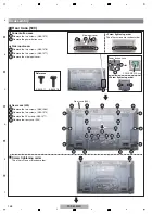
Страница 148: ...he two screws ABA1378 3 Remove the two screws ABA1377 4 Remove the side input cover The other screws are random order The other screws are random order 5 Side input cover Remove the two screws ABA1380 6 Remove the two screws ABA1379 7 Remove the 25 screws ABA1377 8 Remove the rear case 509 9 Rear case 509 Rear case 509 1 1 8 8 8 8 6 7 8 8 8 8 8 8 8 8 8 9 8 8 8 8 8 8 8 8 8 8 8 8 6 7 4 1 1 2 2 3 5 4...

Страница 149: ...eld 2 Side input shield Under cover 509 SIDE IO Assy SIDE HDMI Assy SIDE KEY Assy Screw tightening order 1 1 1 1 1 1 1 1 1 1 1 1 2 4 1 2 2 3 1 3 3 3 2 Remove the 10 screws ABA1377 1 Remove the under cover 509 2 Under Cover 509 3 2 The other screws are random order Screw tightening order The other screws are random order NEVER use an electric screwdriver for tightening this screw Tighten it manuall...

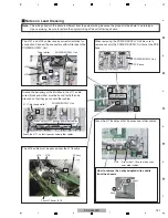
Страница 150: ...y 50F DIGITAL Assy MAIN Assy 1 1 1 1 1 1 1 1 1 1 2 3 3 5 6 7 6 4 6 1 Grip the two short edges of the connector with longnose pliers 2 Insert a finger between the longnose pliers and the board to protect the board and the mounted parts on the board from accidental damage by the pliers then using your finger as a fulcrum and the pliers as a lever pry the connector upward to remove it How to remove t...

Страница 151: ...re correct orientation for connection Connect the connectors with white tape to the POWER SUPPLY Unit Dress so that J111 passes over other cables Pass J215 over J118 Push Pull out 1 2 POWER SUPPLY Unit PCB base When removing the POWER SUPPLY Unit be sure to remove not only the POWER SUPPLY Unit but entire PCB base Around the periphery of the Multibase the J111 cable wires black and white must be b...

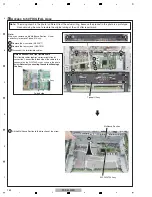
Страница 152: ...ase Section it is not necessary to remove T panel U Assy Note The wiring shown in the photo is different from the actual wiring because the product in the photo is a prototype Upon servicing be sure to restore the original wiring of the unit after repair work Note on connection of the flexible cable This flexible cables requires correct orientation for connection Connect the folded side of the cab...

Страница 153: ...TVU toward you and out 2 Remove the front bezel 509TVU by pulling it upward 3 Front Bezel 509TVU 6 3 2 1 Turn it not to press the rivet Because when the rivet presses fit in once again Rivet Front bezel 509TVU LED Assy IR Assy RLS Assy Front side When assembling the front bezel tighten this rivet first 1 1 1 1 ...

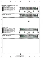
Страница 154: ...ssy 50 4 F Chassis HT Assy 50 F chassis HT Assy 50 1 2 1 2 3 3 4 The other screws are random order 1 2 Screw tightening order Disconnect cables connectors as required 1 Remove the two screws AMZ30P060FTB 2 Remove the two screws ABZ30P080FTC 3 Remove the two screws AMZ30P060FTB 4 Remove the F chassis HB 50 5 F Chassis HB 50 F chassis HB 50 2 3 2 3 4 4 5 The other screws are random order 1 2 Screw t...

Страница 155: ...ssys Sub frame R Assy 50 Sub frame L Assy 50 Sub frame L Assy 50 Sub frame R Assy 50 2 2 3 4 4 2 2 2 1 2 The other screws are random order Screw tightening order 1 2 3 3 2 2 3 2 Remove the 22 screws ABA1351 1 Remove the two address heatsinks S and six address heatsinks L 2 Address heatsink S L Address heatsink S Address heatsink L 1 2 1 3 1 2 1 3 1 3 1 3 1 3 1 3 Address heatsink S Address heatsink...

Страница 156: ...the two screws ABZ30P080FTC 2 Remove the two screws AMZ30P060FTB 3 Remove the F chassis VL Assy 50 4 F chassis VL Assy 50 1 2 3 3 2 4 The other screws are random order 2 1 Screw tightening order 50F Y DRIVE Assy 50F SCAN A Assy 50F SCAN B Assy 50F ADDRESS S Assy 50F ADDRESS L Assy 50F ADDRESS S Assy 50F ADDRESS L Assy ...

Страница 157: ...te Be careful not to bend the Grille Assy too far Otherwise it may be damaged OK Good example NG Bad example Reassembly Remove the old two sided tape attached to the rear side of the Grille Assy and the front side of the baffle and adhere new two sided tape Press the bosses into the baffle plate and press the entire grill into position 2 Woofer Disassembly The woofer is secured to the baffle plate...

Страница 158: ...ore the original settings 3 Use a stable AC power supply Y DRIVE Assy No adjustment required Other assemblies No adjustment required POWER SUPPLY Unit DIGITAL Assy X DRIVE Assy No adjustment required Refer to 8 3 HOW TO CLEAR HISTORY DATA MAIN Assy Execute section 4 5 AUTO ADJUSTMENT of 6 2 4 INITIALIZE Execute section 4 5 AUTO ADJUSTMENT of 6 2 4 INITIALIZE IO AUDIO Assy Service Panel Assy Refer ...

Страница 159: ...ystem IC BCM7404XKPB11G IC7004 EEPROM BR24L64F W IC6201 DDR SDRAM EDD5116AFTA 5B E IC6202 DDR SDRAM EDD5116AFTA 5B E IC6203 DDR SDRAM EDD5116AFTA 5B E IC6204 DDR SDRAM EDD5116AFTA 5B E IC6403 Flash ROM AGC1082 IC6701 Flash ROM AGC1078 IC6811 Flash UCOM AGC1072 IC7202 Flash ROM AGC1073 IC3302 Flash ROM AGC1071 IC3601 Flash UCOM AGC1070 IC8802 EEPROM BR24L01AFJ W PCB Assy No Assy Name Parts that Req...

Страница 160: ...f parts other than those shown in 8 7 ADJUSTMENT WHEN THE MAIN OR IO_AUDIO ASSY IS REPLACED No adjustment is required after replacement of parts other than those shown in 8 7 ADJUSTMENT WHEN THE MAIN OR IO_AUDIO ASSY IS REPLACED No adjustment is required after replacement of parts other than those shown in 8 5 ADJUSTMENT WHEN THE DRIVE ASSYS ARE REPLACED No adjustment required DIGITAL Assy No adju...

Страница 161: ... by lighting the red LED and flashing the blue LED In such a case the adjustment data for backup can be used by copying the data to the EEPROM on the DIGITAL Assy with the following procedures 1 Copying using the Factory menu 1 Turn on the power 2 Enter the Panel Factory mode 3 Display the PANEL INFORMATION page then check if NO DATA is set for DIG EEP and ADJUSTED is set for BACKUP 4 Copy the bac...

Страница 162: ...ION ETC BACKUP DATA NO OPRT Key Down 7th Key Down SET Right SET 5 sec DIGITAL EEPROM NO OPRT DIGITAL EEPROM REPAIR 1 Copying using the Factory menu 1 Turn on the power 2 Enter the Panel Factory mode 3 Display the PANEL INFORMATION page then check if NO DATA is set for DIG EEP 4 Register the changed adjustment data as adjusted data as described for the following procedures then transfer them as bac...

Страница 163: ... check if ADJUSTED is set for DIG EEP 4 Make the data in the EEPROM on the DIGITAL Assy adjustment not completed data by following the procedures below 2 Copying using the RS 232C commands 1 Turn on the power 2 Issue the FAY command 3 With the QS2 command confirm that the main unit adjustment flag is adjustment completed 4 Issue the UAJ command to make the data in the EEPROM on the DIGITAL Assy ad...

Страница 164: ...Turn off the power PANEL INFORMATION ETC BACKUP DATA NO OPRT BACKUP DATA NO OPRT DIGITAL EEPROM NO OPRT PD INFO NO OPRT PD INFO CLEAR Key Down 7th Key Down SET Right SET 5 sec Key Down Key Down Item Content Panel Clearing at the Replacement Clearing method POWER SUPPLY Unit Other parts RS 232C Commands Hour meter Accumulated power on time Must be cleared No need to be cleared No need to be cleared...

Страница 165: ...tment of the panel for service is performed without clearing the pulse meter count proper adjustments will not be performed 2 The drive sequence for Video 60 Hz is used for adjustment When adjustment is made using the Panel Factory menu the current drive sequence is displayed on the screen as shown in the figure below Make sure that 60VS is always indicated during adjustment Example of the On Scre...

Страница 166: ...t 1 3 OK Checking VOL OFFSET max RST MASK 19 Green 626 Recovery flowchart 2 4 OK Checking VOL YNOFSA D max RST MASK 14 Cyan 120 OK Checking VOL YNOFSA D min RST MASK 21 Red 1023 Checking VOL YNOFSA D min RST MASK 22 Green 1023 OK OK Checking VOL YNOFSA D min RST MASK 23 Blue 1023 Recovery flowchart 2 3 OK Recovery flowchart 1 2 OK Checking VOL OFFSET min RST MASK 18 Red 626 Checking VOL YNOFSA D m...

Страница 167: ...amma R value to that for Factory mode PGG S00 To set the gamma G value to that for Factory mode PGB S00 To set the gamma B value to that for Factory mode DIZ S03 Dither ON L dither ON noise OFF 1800000001 LUT mode ON Procedures for resetting corrections for change over time Perform aging for 30 minutes Enter the tentative setting value of the replacement panel Procedures for stabilizing the panel ...

Страница 168: ... MASK 20 Blue 626 MKR S20 Return VOL OFFSET to the tentative setting value VOF Determine the tentative setting value for VOL OFFSET as the final value Yes To the Recovery flowchart 1 3 No Yes To the Recovery flowchart 1 4 From the Recovery flowchart 1 1 and 1 4 Yes No To the Main flowchart 2 Is there erroneous discharge abnormal lit cell Check on the PANEL 1 ADJ menu Is there erroneous discharge a...

Страница 169: ...VOL YNOFS1 D 1 VOL RST P 1 VOL YNOFS3 D 1 VOL XPOFS1 1 VOL YNOFS4 D 1 VOL YNOFS4 A 1 The tentative setting value becomes the final value To the Recovery flowchart 2 1 Yes Is there erroneous discharge abnormal dead cell Check on the PANEL 1 ADJ menu Display RST MASK 23 Blue 1023 MKR S23 Set VOL YNOFSA D to the tentative setting value 162 VYF 162 To the Recovery flowchart 2 4 Yes Is there erroneous ...

Страница 170: ...T to the current setting value plus 106 VOF Replacement of abnormal circuits or re replacement of the panel required No Yes Is there erroneous discharge abnormal dead cell Check on the PANEL 1 ADJ menu Display RST MASK 20 Blue 626 MKR S20 Replacement of abnormal circuits or re replacement of the panel required No Yes Is there erroneous discharge abnormal dead cell Check on the PANEL 1 ADJ menu Rep...

Страница 171: ...rge dead cell The VOL OFFSET value must be 152 or greater Current VOL OFFSET 157 Recovery flowchart 1 3 Changing the VOL OFFSET setting From the Main flowchart 1 Recovery flowchart 1 2 RST MASK 19 Green 626 Display RST MASK 20 Blue 626 MKR S20 To the Recovery flowchart 1 4 To the Recovery flowchart 1 3 Replacement of abnormal circuits or re replacement of the panel required No Yes Gradually decrea...

Страница 172: ...ET to the current setting value minus 106 VOF Gradually decrease the VOL OFFSET value until disappear the discharge dead cell The VOL OFFSET value must be 152 or greater Current VOL OFFSET 157 To the Main flowchart 1 Set VOL OFFSET to the current setting value plus 50 VOF Determine the current VOL OFFSET setting value as the final value Replacement of abnormal circuits or re replacement of the pan...

Страница 173: ...OL YNOFSA D setting From the Main flowchart 2 Replacement of abnormal circuits or re replacement of the panel required No Yes Tentative setting value of VOL YNOFS3 D current setting value of VOL YNOFSA D 254 RST MASK 21 Red 1023 Display RST MASK 22 Green 1023 MKR S22 Gradually increase the VOL YNOFSA D value until disappear the discharge dead cell The tentative setting value of VOL YNOFS3 D curren...

Страница 174: ...eplacement of abnormal circuits or re replacement of the panel required No Yes Tentative setting value of VOL YNOFS3 D current setting value of VOL YNOFSA D 254 Display RST MASK 14 Cyan 120 MKR S14 No Set VOL YNOFSA D to the current setting value minus 34 VYF Determine the current VOL YNOFSA D setting value as the final value Yes Recovery flowchart 2 3 Changing the VOL YNOFSA D setting From the Ma...

Страница 175: ...d 1023 MKR S21 Display RST MASK 22 Green 1023 MKR S22 No Set VOL YNOFSA D to the current setting value plus 23 VYF Determine the current VOL YNOFSA D setting value as the final value Yes Recovery flowchart 2 4 Changing the VOL YNOFSA D setting From the Main flowchart 2 RST MASK 14 Cyan 120 Is there erroneous discharge abnormal dead cell Check on the PANEL 1 ADJ menu Replacement of abnormal circuit...

Страница 176: ...e controls shown in the table below SUS U signal input to the DRIVE Assy SUS B signal input to the DRIVE Assy SUS U signal SUS B signal X DRIVE Gate terminal of Q1219 Y DRIVE Gate terminal of Q2218 X DRIVE Gate terminal of Q1108 Y DRIVE Gate terminal of Q2107 50 of the crest value time lag of SUS U and SUS B Δ Tsus iub time lag of SUS U Gate and SUS B Gate Δ Tsus gub Assy VR Value of α X DRIVE Ass...

Страница 177: ...f Q2111 becomes the same pulse width 5 nsec as the SUS D signal Note For details on measuring points of waveform see the figure below 50 of the crest value 50 of the crest value 50 of the crest value 50 of the crest value SUS D pulse width Tsus Dg Adjust so that Tsus Dg Tsus D 5 nsec using the variable control shown in the table below SUS D signal input to the DRIVE Assy SUS D signal input to the ...

Страница 178: ...iub 60 5 nsec Y DRIVE Assy Y DRIVE Assy 1 Measure the SUS D pulse width Tsus D 2 Adjust the pulse width Tsus Dg of the SUS D input signal so that it becomes Tsus D 5 nsec from DIGITAL Assy YSUS D IC2005_A7 Q2105 VR2001 IC2104 Q2111 IGBT TP2114 Q2113 IGBT TP2116 YSUS U from DIGITAL Assy IC2001_A4 Pin 5 IC2101 IC2103 Q2106 IGBT Q2107 IGBT Q2104 Photo Coupler TP2106 TP2108 Q2109 IGBT Q2108 IGBT TP210...

Страница 179: ...ord Connect the USB memory device Plug in the AC power cord Status AC OFF Screen ON Panel screen ON Panel screen ON Orange LED ON System standby AC OFF AC OFF AC OFF Performing USB updating USB memory device AC OFF AC ON Panel screen OFF Panel screen ON LED LED LED LED LED LED LED NEVER use the remote control unit Especially DO NOT use the Power key If you use any key on the remote control unit in...

Страница 180: ...he DTV software failed Updating of the MAIN microcomputer software failed Updating of the ASIC software in the previous stage failed Updating of the ASIC software in the later stage failed Updating of the module microcomputer software failed Updating of the IF microcomputer software failed Abnormality in the USB memory device The software for a different destination Europe North America Australia ...

Страница 181: ...nces in IC output levels and signal levels upon AD conversion adjustment is performed throughout the path Therefore if any of the following devices is replaced the entire adjustment must be performed again IC8001 AV_SW R2S11006FT IC8101 RGB_SW R2S11001FT IC4702 VDEC CM0048AF IC4801 ADC AD9985KSTZ 110 Perform the AUTO ADJUSTMENT on the 6 2 4 INITIALIZE ...

Страница 182: ...s indicates the importance of the safety factor of the part Therefore when replacing be sure to use parts of identical designation Screws adjacent to b mark on product are used for disassembly For the applying amount of lubricants or glue follow the instructions in this manual In the case of no amount instructions apply as you think it appropriate Falling prevention Metal fittings Screws to Metal ...

Страница 183: ...tructions ARE1488 English French Spanish 9 Caution Card ARM1239 10 Cleaning Caution U ARM1303 11 Power Button Caution ARM1390 NSP 12 Card Register ARY1215 NSP 13 Warranty Card KUC ARY1196 14 Polyethylene Bag AHG1394 15 Paper Angle 509U AHB1301 16 Packing Sheet AHG1405 17 Pad 509 T L U AHA2707 18 Pad 509 T R U AHA2708 19 Pad 509 B L REG AHA2709 20 Pad 509 B R REG AHA2710 21 Upper Carton 5020FD AHD3...

Страница 184: ...184 PDP 5020FD 1 2 3 4 A B C D E F 1 2 3 4 9 2 REAR SECTION POWER SUPPLY P8 IO_AUDIO CN7505 MAIN CN4107 USB MAIN JA4901 HDMI MAIN CN4209 Refer to 9 3 FRONT SECTION ...

Страница 185: ...PCB Spacer AEC1084 15 Edge Saddle AEC1571 16 Mini Clamp AEC1971 17 Inner Grip Assy AMR3693 18 Power Button Support AMR3763 19 USB Gasket ANK1962 20 Power Button Case AAK2927 21 Side Input Cover AMR3754 22 Operation Button AAC1569 23 Power Button 508F AAD4152 24 Rear Case 509 ANE1671 25 Under Cover 509 ANE1672 NSP 26 Name Label 5020FD AAL3029 NSP 27 Serial Seal AAX3182 28 Label A U AAX3566 29 Side ...

Страница 186: ...186 PDP 5020FD 1 2 3 4 A B C D E F 1 2 3 4 9 3 FRONT SECTION MAIN CN4208 MAIN CN4209 Rear view Refer to 9 4 CHASSIS SECTION 1 2 ...

Страница 187: ...RONT SECTION PARTS LIST Mark No Description Part No 1 LED Assy AWW1362 2 IR Assy AWW1363 3 RLS Assy AWW1365 4 7 3 3P Housing Wire J117 ADX3643 5 Front Bezel 509TVU AMB3099 6 Blind Cushion 508F AEB1479 7 Nylon Rivet AEC1671 8 Rivet Plastic AEC1877 ...

Страница 188: ... 1 2 3 4 A B C D E F 1 2 3 4 9 4 CHASSIS SECTION 1 2 FAN CONNECT CN8763 FAN CONNECT CN8762 Cleaning paper GED 008 FAN CONNECT CN8762 FAN CONNECT CN8763 Refer to 9 7 MULTIBASE SECTION Refer to 9 5 CHASSIS SECTION 2 2 ...

Страница 189: ...assis HT Assy 50 ANA2144 7 F Chassis HB 50 ANA2188 8 Waterproof Cushion AEB1495 9 Wire Clip AEC1948 10 Reuse Wire Saddle AEC2134 11 Support Bracket AMR3762 12 FAN Bracket 80 AMR3787 13 Gasket ADH FCH ANK1850 14 Front Gasket V50 ANK1963 15 Front Gasket H50 ANK1964 16 FC Gate Sheet AMR3906 17 Stand Cushion AED1340 18 Screw ABA1313 19 Screw M3 x 6 ABA1377 20 Screw ABZ30P080FTC 21 Screw AMZ30P060FTB 2...

Страница 190: ...IS SECTION 2 2 V D C B A X J H I G F W E Q Q W E S G F D P C O N A M B T O P V S T I J N L K M L K R U U X Z Z MAIN CN4105 CN4101 MAIN CN4202 FAN FAN AC Inlet IO_AUDIO CN7502 MAIN CN4207 MAIN CN4210 POWER SW CN8776 H R Refer to 9 6 PANEL CHASSIS SECTION ...

Страница 191: ...6 ADX3632 21 6P Housing Wire J107 ADX3633 22 5P Housing Wire J108 ADX3634 23 5 3 3P Housing Wire J112 ADX3638 24 5 3 3P Housing Wire J113 ADX3639 25 5 3 3P Housing Wire J114 ADX3640 26 5 3 3P Housing Wire J115 ADX3641 27 6 3 3P Housing Wire J120 ADX3646 28 7 3 3P Housing Wire J121 ADX3647 29 Plate Y 509 ANG3127 30 Nylon Rivet AEC1671 31 Ferrite Core Holder AEC1818 32 Flat Clamp AEC1879 33 Wire Cli...

Страница 192: ...192 PDP 5020FD 1 2 3 4 A B C D E F 1 2 3 4 9 6 PANEL CHASSIS SECTION ...

Страница 193: ...y AWW1350 NSP 5 50F SCAN B Assy AWW1351 NSP 6 P Panel 50F Assy AWU1294 7 Reuse PCB Spacer 4 5 AEC2148 8 Heat Radiation Sheet AEH1134 9 Plate Holder AMR3757 10 Holder L Assy 509 AMR3775 11 Holder S Assy 509 AMR3776 12 Address Plate S 509 ANG3129 13 Address Plate L 509 ANG3130 14 Plate X 509 ANG3128 15 PCB Spacer Reuse AEC2122 16 Address Silicon TS AEH1160 17 Address Silicon TL AEH1161 18 19 20 Scre...

Страница 194: ... B C D E F 1 2 3 4 9 7 MULTIBASE SECTION B B A A RLS CN8736 IR CN8751 SIDE KEY CN8701 LED CN8721 CN3202 CN3201 USB SIDE FAN CONNECT CN8761 HDMI SIDE SIDE IO CN8601 POWER SUPPLY P3 POWER SUPPLY P5 POWER SUPPLY P6 P7 50F DIGITAL ...

Страница 195: ...er AEC1981 24 Reuse PCB Spacer 4 5 AEC2136 or AEC2161 25 PCB Spacer AEC2146 26 HDMI Clamp AEC2147 27 Clamp AEC2156 28 Edge Holder AEC2159 29 Silicon Sheet MTB A AEH1174 30 Silicon Sheet MTB B AEH1175 31 Cable Holder AMR3770 32 Sleeve AMR3771 33 Ether Cover AMR3789 34 MTB Assy ANA2150 35 1 T Panel U Assy ANC2468 36 2 Label B1 U AAX3571 37 2 Label B2 U AAX3582 38 2 Terminal Panel U ANC2463 39 Tuner ...

Страница 196: ...196 PDP 5020FD 1 2 3 4 A B C D E F 1 2 3 4 9 8 PDP SERVICE ASSY Exterior Section PDP SERVICE ASSY 509F AWU1339 Serial Label ...

Страница 197: ...on TL AEH1161 15 Support Bracket AMR3762 16 Gasket ADH FCH ANK1850 17 Front Gasket V50 ANK1963 18 Front Gasket H50 ANK1964 19 Service Pad AEC2105 20 Ferrite Core Holder AEC1818 21 Wire Clip AEC1948 22 Gasket 10 x 10 x 80 ANK1974 NSP 23 Front Service Assy 509 AMB3103 24 Rear Case 509 ANE1671 NSP 25 Drive Voltage Label ARW1097 26 Screw ABA1351 27 Screw ABA1364 28 Screw 3 x 25 P ABA1380 29 Screw ABZ3...

Страница 198: ... F 1 2 3 4 9 9 TABLE TOP STAND TABLE TOP STAND PARTS LIST Front Bottom view Mark No Description Part No 1 Base Cover AXY1176 2 Stand Pipe L AXY1208 3 Stand Pipe R AXY1209 4 Screw ABA1357 5 Screw M8 x 23 ABA1371 6 Screw M8 x 40 ABA1373 ...

Страница 199: ...ene Bag S0 SHL1438 7 1 Speaker Bracket Side SXG1158 8 2 Gasket SED1182 9 2 Gasket SED1183 NSP 10 2 Bracket S SNA1493 11 1 Speaker Bracket Center SXG1159 12 2 Gasket SED1184 13 2 Gasket SED1185 14 2 Gasket SED1186 NSP 15 2 Bracket C SNA1494 16 Protector SIDE SHA2602 17 Protector C T SHA2603 18 Protector C M SHA2604 19 Protector C B SHA2605 NSP 20 Inner Carton Board SHB1192 21 Protection Sheet S1 SH...

Страница 200: ... D E F 1 2 3 4 9 11 SPEAKER SYSTEM Baffle back Grille back Top Rear Top Tweeter Input Terminal Input Terminal Section A Baffle Front Grille Front Top Top Cabinet inside Inside Section B Outside WF TW TW WF TW WF TW WF WF WF TW TW ...

Страница 201: ...et SEC2203 NSP 17 Gasket SEC2204 NSP 18 Gasket SEC2205 NSP 19 Gasket SEC2229 NSP 20 Gasket SEC2235 NSP 21 Felt SED1127 NSP 22 Felt SED1130 23 Tape SEH1089 24 Tape SEH1099 25 Tape SEH1115 26 Input Terminal SKX1098 NSP 27 MDF Bar SLX1176 NSP 28 Paper Tube 26 SMR1403 NSP 29 Acoustic Absorbent SMT1328 NSP 30 Acoustic Absorbent SMT1331 NSP 31 Acoustic Absorbent SMT1333 NSP 32 Acoustic Absorbent SMT1335...

Отзывы: