background image

 Pin 

Description 


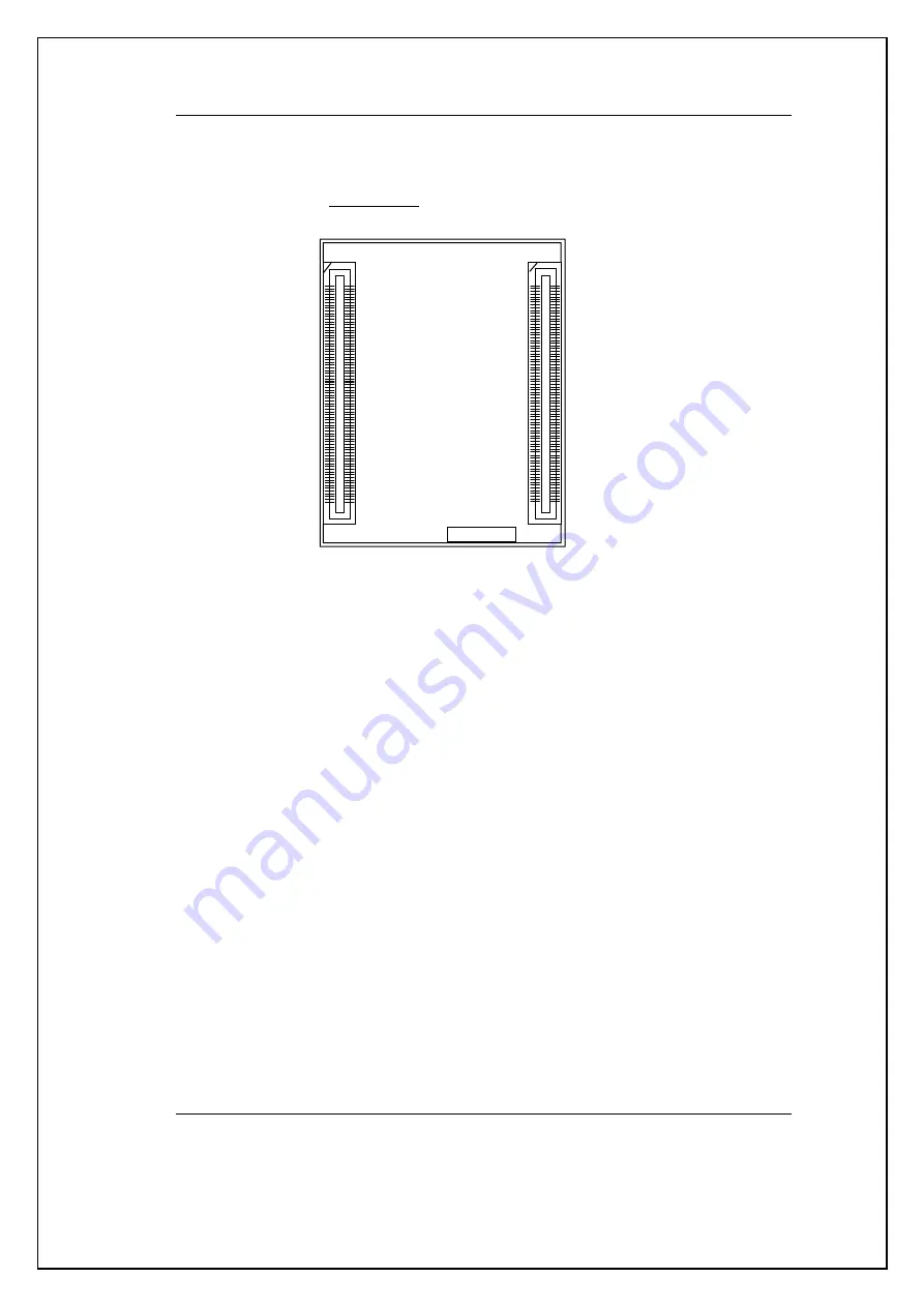
The following figure (

Figure 4

) illustrates the numbered matrix 

system. It shows a phyCORE-TC1796 with SMT phyCORE-
connectors on its underside.
 

Figure 4: 

Pinout of the phyCORE-Connector (view from Connector Side) 

 
Many of the controller port pins accessible at the connectors along the 
edges of the board have been assigned alternate functions that can be 
activated via software. 


©

 PHYTEC Meßtechnik GmbH 2009     L-719e_2 

11


D  C 

X3


B A

X3

80 

80 

1

1

80

80

Содержание phyCORE-TC1796

Страница 1: ...A product of a PHYTEC Technology Holding company phyCORE TC1796 Hardware Manual Edition May 2009...

Страница 2: ...TEC Messtechnik GmbH offers no guarantee nor accepts any liability for damages arising from the improper usage or improper installation of the hardware or software PHYTEC Messtechnik GmbH further rese...

Страница 3: ...dard Flash 35 7 Serial Interfaces 36 7 1 RS 232 Interface U5 36 7 2 CAN Interface 38 7 3 On Chip Debug Support OCDS1 39 7 4 USB to UART Bridge U10 42 8 Hardwired TCP IP Ethernet Controller U21 43 8 1...

Страница 4: ...7 Figure 3 View of the phyCORE TC1796 Connector Side 8 Figure 4 Pinout of the phyCORE Connector view from Connector Side 11 Figure 5 Numbering of the Jumper Pads 22 Figure 6 Location of the Jumpers C...

Страница 5: ...Contents PHYTEC Me technik GmbH 2009 L 719e_2 Index of Tables Table 1 Pinout of the phyCORE Connector X3 21 Table 2 Jumper Settings 28 Table 3 Runtime Memory Map 34 Table 4 OCDS1 Connector X1 Pin Assi...

Страница 6: ......

Страница 7: ...phyCORE TC1796 PHYTEC Single Board Computers henceforth products are designed for installation in electrical appliances or as dedicated Evaluation Boards i e for use as a test and prototype platform f...

Страница 8: ...ould ensure conformance following any modifications to the products as well as implementation of the products into target systems The phyCORE TC1796 is one of a series of PHYTEC Single Board Computers...

Страница 9: ...s stem from insufficient supply voltage grounding of electronic components in high frequency environments the phyCORE board design features an increased pin package The increased pin package allows de...

Страница 10: ...oller to high density pitch 0 635 mm connectors aligning two sides of the board allowing it to be plugged like a big chip into a target application Precise specifications for the controller populating...

Страница 11: ...cal Timer Cell Array LTCA2 Two 16 channel Analog to Digital Converter units ADC with selectable 8 bit 10 bit or 12 bit resolution One 4 channel Fast Analog to Digital Converter unit FADC 44 analog inp...

Страница 12: ...phyCORE TC1796 Operating temperature 40 C to 85 C 1 1 Block Diagram 6 PHYTEC Me technik GmbH 2009 L 719e_2 Figure 1 Block Diagram phyCORE TC1796...

Страница 13: ...Introduction 1 2 View of the phyCORE TC1796 PHYTEC Me technik GmbH 2009 L 719e_2 7 Figure 2 View of the phyCORE TC1796 Controller Side...

Страница 14: ...phyCORE TC1796 8 PHYTEC Me technik GmbH 2009 L 719e_2 Figure 3 View of the phyCORE TC1796 Connector Side...

Страница 15: ...d to as phyCORE connector This allows the phyCORE TC1796 to be plugged into any target application like a big chip A new numbering scheme for the pins on the phyCORE connector has been introduced with...

Страница 16: ...wed from above even if all connector contacts extend to the bottom of the module The numbering scheme is thus consistent for both the module s phyCORE connector as well as mating connectors on the phy...

Страница 17: ...nnectors on its underside Figure 4 Pinout of the phyCORE Connector view from Connector Side Many of the controller port pins accessible at the connectors along the edges of the board have been assigne...

Страница 18: ...O Microcontroller s Chip Select output Used for onboard Ethernet Controller U21 Free to use if the U21 is NOT populated or jumper J24 is open refer to jumper J24 6A ADV O Microcontroller s Address Va...

Страница 19: ...t P1 13 56A P111 I O Microcontroller s port P1 11 58A P18 I O Microcontroller s port P1 8 59A P17 I O Microcontroller s port P1 7 60A P16 I O Microcontroller s port P1 6 61A P14 I O Microcontroller s...

Страница 20: ...to jumper J18 6B CS1 I O Microcontroller s Chip Select signal Used for first onboard SRAM BANK U17 U18 Free to use if the first RAM Bank is NOT populated or Jumper J17 is open refer to jumper J17 7B x...

Страница 21: ...1 5 61B P13 I O Microcontroller s port P1 3 62B P315 I O Microcontroller s port P3 15 63B P313 I O Microcontroller s port P3 13 65B P310 I O Microcontroller s port P3 10 66B P38 I O Microcontroller s...

Страница 22: ...ble If S1 is populated default because the pads of these jumpers are below DIP switchS1 refer to jumper J3 J10 Use Dip switch S2 to configure SWOPT0 7 10C HDRST I O Microcontroller s hard reset signal...

Страница 23: ...l interface Alternative port P6 4 29C SCLK1 I O SSC1 clock input output of the 2nd TC1796 synchronous serial interface Alternative port P 6 6 30C 5V_VBUS I USB VBUS 5V input for opt bus powered USB to...

Страница 24: ...orts to the phyCORE connector X3 Alternative Microcontroller s P57 Alternative Microcontroller s P9 8 Alternative Microcontroller s P9 6 Alternative Microcontroller s P9 4 Alternative Microcontroller...

Страница 25: ...TXD0_TTL O Transmit line of first TC1796 UART Alternative port P5 1 18D CAN_L1 I O CANL output of the CAN transceiver for the 2nd TC1796 CAN node Alternative port 6 10 refer to jumper J42 20D CAN_L0 I...

Страница 26: ...er controller U11 33D IRQRTC O RTC interrupt output 35D E_RX I RxD input of the Ethernet Controller U21 36D E_TX O TxD output of the Ethernet Controller U21 37D D I O USB D data line from opt bus powe...

Страница 27: ...yCORE connector X3 Alternative P9 7 Alternative P9 5 Alternative P9 3 Alternative P9 2 Alternative P4 13 Alternative P4 12 Alternative P4 10 Alternative P4 7 Alternative P4 5 Alternative P4 4 Alternat...

Страница 28: ...prior to delivery Figure 5 illustrates the numbering of the jumper pads while Figure 6 and indicate the location of the jumpers on the module 1 2 3 e g J20 1 2 3 4 e g J29 1 2 e g J3 1 2 open closed...

Страница 29: ...Jumpers PHYTEC Me technik GmbH 2009 L 719e_2 23 Figure 7 Location of the Jumpers Connector Side...

Страница 30: ...Bootconfig Following a power on reset PORST If BOOT high Boot config Via J 7 10 HWCFG 0 3 access to J3 J6 only available if S1 is NOT populated open Signal is GND closed Signal is 3V3 footprint 0R SMD...

Страница 31: ...on X3 closed X CS1 is connected to the onboard SRAM BANK1 U17 U18 footprint 0R SMD 0805 J18 Connects the MCU s CS2 output to the onboard SRAM BANK2 memory U19 U20 open X CS2 is freely usable on X3 clo...

Страница 32: ...PHYTEC Me technik GmbH 2009 L 719e_2 J26 Connects P1 14 to microSD card slot for card detect closed X P1 14 connected and used as card detect open P1 14 not connected and NOT used as card detect foot...

Страница 33: ...must be unpopulated to use this configuration footprint 0R SMD 0805 J32 J34 Roote the signals of the second ASC Interface ASC1 1 2 1 2 X Port P5 3 und P5 2 are connected to the RS232 driver U5 2 3 2...

Страница 34: ...rd CAN transceivers must not be populated Footprint 0R SMD 0805 J45 J47 These jumpers configure the correct byte control signals being used on the MCU depending on the SRAM devices SRAM BANK1 U17 U18...

Страница 35: ...Jumpers PHYTEC Me technik GmbH 2009 L 719e_2 29...

Страница 36: ...ly one supply voltage Supply voltage 3 3 V 5 max 1200mA typ 400mA Once all voltages have reached their target level the voltage supervisory circuit keeps the PORST reset signal at low level low is the...

Страница 37: ...e TC1796 implements two basic booting schemes a hardware booting scheme that is invoked through external pins and a software booting scheme in which software can determine the boot options overriding...

Страница 38: ...ind read from address 0x000004 of the memory device attached to CS0 in order to read the EBU boot configuration word 32Bit see section 13 4 3 of the TC1796 Systems Units Manual This first read access...

Страница 39: ...memory model is configured via software using the internal registers of the TC1796 There is a register set containing a BUSCON BUSAP and ADDSEL register for each of the controllers Chip Select signals...

Страница 40: ...DRSEL0 0xA4000833 EBU_BUSCON0 0x00922200 EBU_BUSAP0 0x80D81D00 0xA0000000 0xA03FFFFF 4 MB on board SRAM CS1 or free available EBU_ADDRSEL1 0xA1000853 EBU_BUSCON1 0x00820000 EBU_BUSAP1 0x45B80000 0xA80...

Страница 41: ...sh at U3 and U4 CS0 is connected to the Flash memory bank With this configuration this memory bank is active following power on reset 6 3 1 Standard Flash The Intel PC28F640JV3D75 is the standard Flas...

Страница 42: ...t handshake signal communication However depending on user needs hand shake communication can be software emulated using port pins on the microcontroller Use of an RS 232 signal level in support of ha...

Страница 43: ...e CPU internal This means that you could choose via configuration register which port Pins are used Jumper J31 J32 J33 J34 must be set according to your configuration in order to connect the right pin...

Страница 44: ...VD23x 2 VDC 7 VDC If the CAN bus system exceeds these limiting values optical isolation of the CAN signals is required For larger CAN bus systems an external opto coupler should be implemented to galv...

Страница 45: ...s via the JTAG interface The OCDS1 JTAG interface on the TC1796 extends to the phyCORE connector X3 and a 16 pin 2mm pitch connector at X1 refer to table4 for Pin Assignment located on the edge of the...

Страница 46: ...phyCORE TC1796 Figure 8 OCDS1 JTAG interface X1 connector side 40 PHYTEC Me technik GmbH 2009 L 719e_2 X1 Pin1 on connector bottom side...

Страница 47: ...3 JTAG module serial data output GND 44D 4 Ground GND 37C 6 Ground TDI 40D 7 JTAG module serial data input PORST 11C 8 Power on reset input TRST 41C 9 JTAG module reset enable input BRKOUT 40C 10 OCD...

Страница 48: ...onnected to communicate over USB to a Host PC This is done by closing jumper J12 and J13 open per default so that RxD0 P5 0 of the TC1796 is connected to the UART Transmit of CP2102 and TxD0 P5 1 of t...

Страница 49: ...of the W5300 for information how to initialize and program the Ethernet interface Also refer to the datasheets of the W5300 for the needed Transformer characteristics 8 1 MAC Address In a computer ne...

Страница 50: ...nd its content of a stored MAC address in the SPI EEPROM Every position of the MAC address is stored as a binary value in the SPI EEPROM MAC address Example 0050C2A0C093 SPI EEPROM address Stored Byte...

Страница 51: ...ming Because the phyCORE TC1796 has populated two of IIC BUS Master Controller it provides the Signals for two independent IIC Buses on the phyCORE connector at X3C31 X3D32 SCL0 SDA0 and X3C25 X3C24 S...

Страница 52: ...n data or operating parameters that must not be lost in the event of a power interruption Depending on the module s configuration this memory can be in the form of an EEPROM per default or FLASH with...

Страница 53: ...VDC voltage at Pin X3C6C VBAT_IN the Real Time Clock runs independently of the board s power supply Programming the Real Time Clock is done via the first IIC U11 Interface controller SCL0 SDA0 The I2C...

Страница 54: ...g a battery via the VBAT_IN input is not mandatory for normal operation of the module since all devices listed above are supplied with power by the module s operating voltage 3V3 13OCDS2 debugging The...

Страница 55: ...e microSD is connected to the Microcontroller s SSC1 interface using SLSO7 SSC Slave Select Output 7 for the microSD Furthermore Port Pin input P1 14 is used to as card detect input If a microSD is in...

Страница 56: ...igure 9 The module s profile is ca 7 mm thick with a maximum component height of 2 mm on the backside of the PCB and approximately 3 mm on the top side The board itself is approximately 2 mm thick Fig...

Страница 57: ...andard 40 C to 9085 C except ethernet W5300 0 C to 80 C Humidity 95 r F not condensed Operating voltages 3 3 V 5 VBAT 3 V 5 Power consumption 3 3 V voltage Conditions 150 MHz clock 4 MByte LP RAM 1 MB...

Страница 58: ...tes the distance between the two connected PCBs when the module is mounted on the corresponding carrier board In order to get the exact spacing the maximum component height 2 mm on the underside of th...

Страница 59: ...r a few alternations components can be removed with the solder iron tip Alternatively a hot air gun can be used to heat and loosen the bonds Integrating the phyCORE TC1796 in application circuitry Suc...

Страница 60: ...Manual L 719e_1 KSP 0150 1 PCB PL2197 1 1st edition 29 May 2009 Manual L 719e_2 KSP 0150 1 PCB PL2197 1 2nd edition change J18 open per default correction on page19 CAN_H0 is Port 6 9 MAC address stor...

Страница 61: ...ase Notes The following paragraph describes the differences between the technical facts provided in this manual and the currently available hardware revisions phyCORE TC1796 modules with PCB number PL...

Страница 62: ...51 J JTAG 39 Jumper Settings 28 M MAC Address 43 Memory Model following Reset 33 Runtime 33 Memory Models 33 O OCDS 39 Operating Temperature 6 51 Operating Voltage 51 P phyCORE connector 9 12 Physical...

Страница 63: ...Suggestions for Improvement PHYTEC Me technikGmbH 2009 L 719e_2 T Technical Specifications 50 U U13 46 U5 36 UART on chip 36 W Weight 51...

Страница 64: ...E TC1796 Document number L 719e_2 May 2009 How would you improve this manual Did you find any mistakes in this manual page Submitted by Customer number Name Company Address Return to PHYTEC Technologi...

Страница 65: ...Published by PHYTEC Me technik GmbH 2009 Ordering No L 719e_2 Printed in Germany...

Отзывы: