2.5
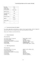
ESD Requirements
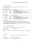
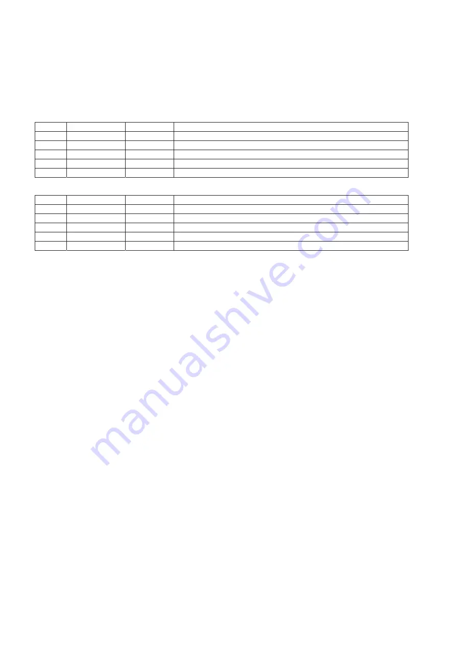
The product shall withstand electro static discharges on all user accessible parts of the product.
Reference: IEC61000-4-2.
For contact discharges:
Level General
(kV) USA
(kV) Requirement
1 0-2
0-3
No
deviations
allowed.
2
>2-4
>3-4
Short perceptible deviations allowed
3 >4-5
>4-5 Normal
recallable
functions function changes allowed.
4 >5-7
>5-7 Control
recallable
functions function changes allowed.
5
-
>7-8
No loss of stored data allowed.
For air discharge:
Level General
(kV) USA
(kV) Requirement
1 0-4
0-6
No
deviations
allowed.
2
>4-8
>6-8
Short perceptible deviations allowed.
3 >8-10
>8-10 Normal
recallable
functions function changes allowed.
4
>10-15
>10-15
Control recallable functions function changes allowed.
5
-
>15-18
No loss of stored data allowed.
General requirement:
1. 10 arcs for positive and negative polarity for unit “on” and “off” for 1kV incremental steps.
2. Component or mechanical damage is not allowed. No loss of fixed stored data (stored in EEPROMs).
3. Hang-ups and malfunctions are allowed, as long as the customer can “recover” from the hang-up by
pressing the Standby or ON/OFF button of the set.
4. Failures that disappear only by unplugging the AC mains cord and/or power sources are not acceptable.
2.6
Environmental Condition
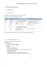
The environmental condition requirements and test method is according to UAN-D1590.
Ambient temperature
: max. 40 ° C - all climates
Apparatus acc. to spec.
: +5 to + 35 ° C
Vibration test (acc. IEC 60 068/2/6) : operational vibration test to be proceeded in operating position of the
set.
2.7
Quality
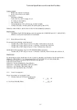
PQR-class: class 2 according to BLC A&MA PQR handbook V2.1 (2006-10-02)
Lifetime: 7 years
Tested According to: General Test Instruction UAN-D 1591
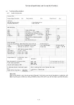
Measured According to: UAN_L 1059 unless otherwise stated
Technical Specification and Connection Facilities
1-5
Содержание MCD2010/12/93
Страница 26: ...8 2 Fig D4 Cabinet Disassembly Instructions ...
Страница 33: ...Display Board Layout Diagram 12 3 12 3 ...
Страница 35: ...Power Board Layout Diagram 12 5 12 5 ...
Страница 42: ...Decoder Board Layout Diagram 12 12 12 12 ...
Страница 43: ...Exploded View PCB1 S001 S005 PCB4 PCB2 Bottom Chassis S002 S004 S007 S006 PCB5 PCB3 DVDM Top Cabinet 13 1 13 1 ...
Страница 44: ...Revision List Revision List Version 1 0 Initial Release 14 1 ...


