Memory Accelerator Module (MAM)
71
Philips Semiconductors
Preliminary User Manual
LPC2119/2129/2292/2294
ARM-based Microcontroller
Flash programming operations are not controlled by the Memory Accelerator Module, but are handled as a separate function. A
“boot block” sector contains Flash programming algorithms that may be called as part of the application program, and a loader
that may be run to allow serial programming of the Flash memory.
The Flash memories are wired so that each sector exists in both banks, such that a sector erase operation acts on part of both
banks simultaneously. In effect, the existence of two banks is transparent to the programming functions.
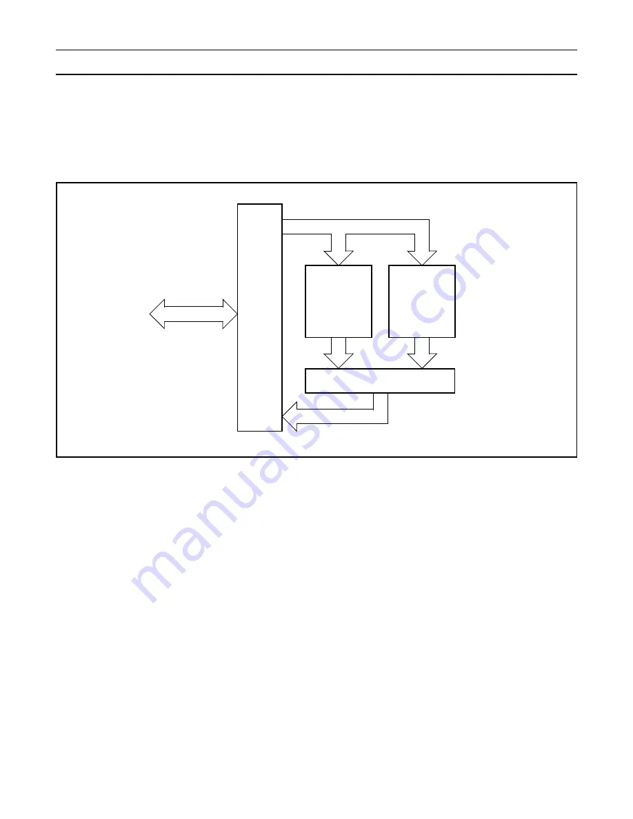
Figure 17: Simplified Block Diagram of the Memory Accelerator Module
Instruction Latches and Data Latches
Code and Data accesses are treated separately by the Memory Accelerator Module. There are two sets of 128-bit Instruction
Latches and 12-bit Comparison Address Latches associated with each Flash Bank. One of the two sets, called the Branch Trail
Buffer, holds the data and comparison address for that bank from the last Instruction miss. The other set, called the Prefetch
Buffer, holds the data and comparison address from prefetches undertaken speculatively by the MAM. Each Instruction Latch
holds 4 words of code (4 ARM instructions, or 8 Thumb instructions).
Similarly there is a 128-bit Data Latch and 13-bit Data Address latch, that are used during Data cycles. This single set of latches
is shared by both Flash banks. Each Data access that is not in the Data latch causes a Flash fetch of 4 words of data, which are
captured in the Data latch. This speeds up sequential Data operations, but has little or no effect on random accesses.
Flash Programming Issues
Since the Flash memory does not allow accesses during programming and erase operations, it is necessary for the MAM to force
the CPU to wait if a memory access to a Flash address is requested while the Flash module is busy. (This is accomplished by
asserting the ARM7TDMI-S local bus signal CLKEN.) Under some conditions, this delay could result in a Watchdog time-out. The
user will need to be aware of this possibility and take steps to insure that an unwanted Watchdog reset does not cause a system
failure while programming or erasing the Flash memory.
Flash Memory
Bank 0
Flash Memory
Bank 1
Bank
Selection
Bus
Interface
Memory Address
Memory Data
ARM Local Bus


