background image

1-9-5

E5J10TR

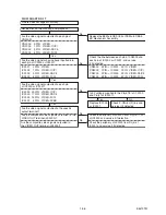
Is 5V voltage supplied to the Pin(4,18) of IC2300 
and Pin(4) of IC2301?

Replace IC2300 
or IC2301.

Check P-ON+5V(2) line and
service it if detective.

Are the video signals outputted to each pin 
of IC2300 or IC2301?

Yes

No

Yes

Yes

No

IC2300   20PIN    VIDEO-Y(I/P)
IC2300   17PIN    VIDEO-Pb/Cb
IC2300   15PIN    VIDEO-Pr/Cr
IC2301     5PIN    VIDEO-CVBS

Check the periphery of JK2300 from Pin(15,17,20) 
of IC2300 and service it if detective.

Check the periphery of JK2300 from Pin(5) of 
IC2301 and service it if detective.

Are the video signals outputted to the specific 
output terminal?

Are the component video signals outputted to the 
VIDEO OUT terminal (JK2300)?

No

No

Are the composite video signals outputted to 
the VIDEO OUT terminal (JK2300)?

FLOW CHART NO.17

Picture does not appear normally. 

Set the disc on the disc tray, and playback.

Are the video signals outputted to each pin of 
CN2000?

Replace the BE Main CBA Unit or FE Main CBA &  
BD Mechanism Assembly.

Check the line between each pin of CN2000 and 
each pin of IC2300 or IC2301, and service  
it if detective.

CN2000    9PIN 

 IC2301    3PIN   VIDEO

CN2000    1PIN 

 IC2300    1PIN   VIDEO-Y(I/P)

CN2000    3PIN 

 IC2300    3PIN   VIDEO-Pb/Cb

CN2000    5PIN 

 IC2300    5PIN   VIDEO-Pr/Cr

Are the video signals shown above inputted into 
each pin of IC2300 or IC2301?

Yes

No

No

CN2000     9PIN    VIDEO
CN2000     1PIN    VIDEO-Y(I/P)
CN2000     3PIN    VIDEO-Pb/Cb
CN2000     5PIN    VIDEO-Pr/Cr

IC2301     3PIN    VIDEO
IC2300     1PIN    VIDEO-Y(I/P)
IC2300     3PIN    VIDEO-Pb/Cb
IC2300     5PIN    VIDEO-Pr/Cr

Содержание BDP7200/12

Страница 1: ...indhoven The Netherlands All rights reserved No part of this publication may be reproduced stored in a retrieval system or transmitted in any form or by any means electronic mechanical photocopying or otherwise without the prior permission of Philips CLASS 1 LASER PRODUCT KLASSE 1 LASER PRODUKT KLASS 1 LASER APPARAT CLASSE 1 PRODUIT LASER 12NC 3139 785 34350 Service Manual Service Service Service ...

Страница 2: ... each way Consequently Philips has not undertaken any such broad evaluation Accordingly a servicer who uses a service procedure or tool which is not recommended by Philips must first use all precautions thoroughly so that neither his safety nor the safe operation of the equipment will be jeopardized by the service method selected TABLE OF CONTENTS LASER BEAM SAFETY PRECAUTIONS 1 1 1 IMPORTANT SAFE...

Страница 3: ...away from the pickup lens when the diode is turned on Do not look directly at the laser beam CAUTION Use of controls and adjustments or doing procedures other than those specified herein may result in hazardous radiation exposure Location Inside Top of BD mechanism Do not look directly at the laser beam coming from the pickup or allow it to strike against your skin Drive Mechanism Assembly Laser B...

Страница 4: ...ical for safety Replace only with part number specified B In addition to safety other parts and assemblies are specified for conformance with regulations applying to spurious radiation These must also be replaced only with specified replacements Examples RF converters RF cables noise block ing capacitors and noise blocking filters etc C Use specified internal wiring Note especially 1 Wires covered...

Страница 5: ...le parts RF termi nals antenna terminals video and audio input and output terminals microphone jacks earphone jacks etc is lower than or equal to the specified value in the table below Measuring Method Power ON Insert load Z between B earth ground power cord plug prongs and exposed accessible parts Use an AC voltmeter to measure across the terminals of load Z See Fig 2 and the following table AC L...

Страница 6: ...only lead free solder alloy Philips SAC305 with order code 0622 149 00106 If lead free solder paste is required please contact the manufacturer of your solder equipment In general use of solder paste within workshops should be avoided because paste is not easy to store and to handle Use only adequate solder tools applicable for lead free solder alloy The solder tool must be able To reach at least ...

Страница 7: ...nd other ICs used in Philips sets You will find this and more technical information within the magazine chapter workshop news For additional questions please contact your local repair helpdesk How to Remove Install Flat Pack IC 1 Removal With Hot Air Flat Pack IC Desoldering Machine 1 Prepare the hot air flat pack IC desoldering machine then apply hot air to the Flat Pack IC about 5 to 6 seconds F...

Страница 8: ... solder flux which is applied to all pins of the flat pack IC you can remove it easily Fig S 1 3 2 Affix the wire to a workbench or solid mounting point as shown in Fig S 1 5 3 While heating the pins using a fine tip soldering iron or hot air blower pull up the wire as the solder melts so as to lift the IC leads from the CBA contact pads as shown in Fig S 1 5 4 Bottom of the flat pack IC is fixed ...

Страница 9: ...cur due to a potential difference caused by electrostatic charge during unpacking or repair work 1 Ground for Human Body Be sure to wear a grounding band 1 MΩ that is properly grounded to remove any static electricity that may be charged on the body 2 Ground for Workbench Be sure to place a conductive sheet or copper plate with proper grounding 1 MΩ on the workbench or other surface where the semi...

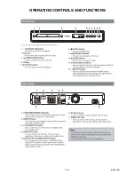
Страница 10: ...1 4 1 E5J10IB OPERATING CONTROLS AND FUNCTIONS ...

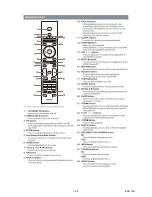
Страница 11: ...1 4 2 E5J10IB ...

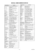
Страница 12: ... Front Audio Mute Right Signal Mute L GND Ground IIC BUS SCL IIC BUS Serial Clock IIC BUS SDA IIC BUS Serial Data KEY 1 Key Data Input 1 MAIN P ON Power On Signal MODE1 Mode 1 Signal MODE2 Mode 2 Signal OSC1 Main Clock Output OSC2 Main Clock Input P ON 1 2V 1 2V at Power On Signal P ON 10 5V 10 5V at Power On Signal P ON 12V 12V at Power On Signal P ON 3 3V 3 3V at Power On Signal P ON 5V 5V at Po...

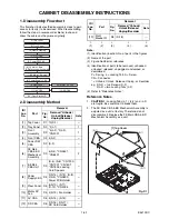
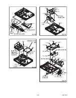
Страница 13: ... at factory Therefore do not disassemble it Replace the FE Main CBA BD Mechanism Assembly as a unit ID Loc No Part Removal Fig No Remove Unhook Unlock Release Unplug Desolder Note 1 Top Cover D1 10 S 1 2 Tray Panel D2 2 L 1 1 3 Front Assembly D2 5 L 2 3 L 3 CN2001 1 4 Front CBA D2 4 S 2 5 Power SW CBA D2 S 3 6 FE Main CBA BD Mechanism Assembly D3 4 S 4 CN2601 CN6401 2 7 BE Main CBA Unit D3 S 5 S 6...

Страница 14: ...Main CBA BD Mechanism Assembly CN7000 CN7001 CN7401 CN2601 CN7602 CN6401 S 6 S 5 Locking Card Spacers S 4 Fig D3 Fig D4 8 Power Supply CBA S 8 CN2600 Power PCB Holder S 9 S 7a S 7a S 7b 11 AV CBA 9 Rear Panel 12 SD CBA S 18 S 16 S 17 S 17 SD Card Holder S 15 S 14 S 14 CN2004 S 14 10 Motor DC Fan Fan Holder 13 Front Bracket R S 10 S 12 S 13 S 11 Wire Wire Fig D5 ...

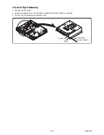
Страница 15: ...w to Eject Manually 1 Remove the Top Cover 2 Insert a screwdriver etc into the Hole A straightly so that the Portion A is pushed 3 Pull the tray out manually and remove a disc Screwdriver hexagon wrench Hole A Portion A ...

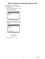
Страница 16: ... control unit in that order Fig a appears on the screen 3 Press STOP button on the remote control unit Fig b appears on the screen and Fig c appears on the VFD 4 To exit this mode press button Fig a differ depending on the models Model Name Version Region Version Info EXIT POWER EEPROM CLEAR STOP Fig b differ depending on the models Model Name Version Region Version Info EXIT POWER EEPROM CLEAR ST...

Страница 17: ...is time no button is available 6 Unplug the AC cord from the AC outlet Then plug it again 7 Turn the power on 8 Press 1 2 3 4 and INFO buttons on the remote control unit in that order Fig g appears on the screen F W VERSION UP MODE Model No Ver Please insert a Disc for F W Version Up differs depending on the models Fig a Version Up Mode Screen Fig b VFD in Version Up Mode 1 ALL Now Loading Ver B b...

Страница 18: ... 1 Turn the power on 2 Press 1 2 3 4 and INFO buttons on the remote control unit in that order Fig j appears on the screen 3 To exit this mode press button Fig h differ depending on the models Model Name Version Region Version Info EXIT POWER EEPROM CLEAR STOP EEPROM CLEAR OK Fig i Fig j differ depending on the models Model Name Version Region Version Info EXIT POWER EEPROM CLEAR STOP ...

Страница 19: ...r periphery and service it if defective Check IC1003 D1009 and their periphery and service it if defective FLOW CHART NO 5 FL is not outputted Is 34 5V voltage supplied to the emitter of Q2012 Check D1018 C1021 and periphery circuit and service it if defective Check FL SW line and service it if defective Is the L signal outputted to the collector of Q2013 Yes Yes Yes No No No FLOW CHART NO 1 The p...

Страница 20: ...6 P ON 12V is not outputted Is 12V voltage supplied to the emitter of Q2603 Is the voltage of base on Q2603 lower than the voltage of emitter on Q2603 when turning the power on Replace Q2603 Check D1011 D1019 C1017 L1005 and their periphery circuit and service it if defective Check Q2601 and PWSW3 line and service it if defective Yes Yes No No Is the voltage of base on Q2606 lower than the voltage...

Страница 21: ...e remote control unit is activated Is the H pulse inputted to the Pin 27 of IC2000 Replace IC2000 Is 5V voltage supplied to Pin 2 of RS3000 remote control receiver Yes No Check AL 3 3V line and service it if defective No No Yes Yes Yes Yes Yes No Yes No Yes No No No FLOW CHART NO 12 The fluorescent display tube does not light up Is 3 3V voltage supplied to Pin 24 of FL3000 Is 8V voltage supplied t...

Страница 22: ...or Replace the FE Main CBA BD Mechanism Assembly No improvement can be found No Yes FLOW CHART NO 15 The disc tray cannot be opened and closed It can be done using the remote control unit Is the normal control voltage inputted to Pin 4 of IC2000 Refer to FLOW CHART NO 13 The key operation is not functioning Refer to FLOW CHART NO 16 The disc tray cannot be opened and closed Replace the OPEN CLOSE ...

Страница 23: ... OUT terminal JK2300 No No Are the composite video signals outputted to the VIDEO OUT terminal JK2300 FLOW CHART NO 17 Picture does not appear normally Set the disc on the disc tray and playback Are the video signals outputted to each pin of CN2000 Replace the BE Main CBA Unit or FE Main CBA BD Mechanism Assembly Check the line between each pin of CN2000 and each pin of IC2300 or IC2301 and servic...

Страница 24: ...CBA Unit or FE Main CBA BD Mechanism Assembly Replace the BE Main CBA Unit or FE Main CBA BD Mechanism Assembly Replace IC2200 Check the periphery between Pin 1 7 of IC2200 and JK2200 and service it if detective Check each line between each pin of CN2000 and each pin of IC2200 and service it if detective CN2000 27PIN IC2200 6PIN AUDIO L CN2000 25PIN IC2200 2PIN AUDIO R Are the analog audio signals...

Страница 25: ...IN IC2701 2 6PIN CENTER SUB WOOFER CN2701 7 9PIN IC2702 2 6PIN SURROUND L R Are the analog audio signals inputted to each pin of IC2700 IC2701 and IC2702 Are the analog audio signals outputted to each pin of IC2700 IC2701 and IC2702 IC2700 1 7PIN FRONT AUDIO L R IC2701 1 7PIN CENTER SUB WOOFER IC2702 1 7PIN SURROUND L R Yes Yes No No No Check each line and service it if defective No Replace the BE...

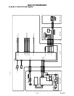
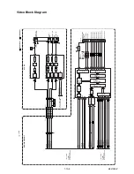
Страница 26: ...SDA IIC BUS SCL IIC BUS SDA PWSW2 PWSW3 A33 PW CONT STANDBY LED SYS RESET RDY RDY B18 TXD1 G18 A18 A17 RXD1 SCL SDA SCL SDA FL SDA FL SCL FL CS REMOTE KEY 1 OSC2 OSC1 8MHz X TAL X2000 EV 3 3V IC2001 RESET D 3 3V D 3 3V Q2003 BUFFER Q7501 JK7501 Q6702 Q6703 Q6701 26 FL SW FL SW TO POWER SUPPLY BLOCK DIAGRAM TO VIDEO BLOCK DIAGRAM 31 AUDIO MUTE AUDIO MUTE 45 FAN CONT FAN CONT 50 V5V PW SW V5V PW SW ...

Страница 27: ...Q AG28 AH4 AG5 U4 U3 T2 R3 T1 R4 AA1 Y3 K4 100 125 128 AH29 AH28 AH30 2 4 7 9 10 11 12 13 14 SLD2 4 SLD2 3 SLD1 2 SLD1 1 CN902 LOAD 5 LOAD 6 LDSNS1 2 LDSNS2 1 CN901 TD 3 TR 4 FD1 1 FR1 2 EXPA 9 EXPA 7 EXPB 10 EXPB 8 A D 21 24 E H 26 29 OEVC 25 RF 17 RF 18 BDRF 14 BDRF 15 SDATA 40 SCLK SDATA SCLK SDATA SCLK 38 CN101 CN101 15 16 17 18 14 13 12 11 14 13 15 16 LOADING MOTOR DRIVE 10 9 COLLIMATE LENS M...

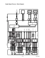
Страница 28: ... SDCLK DDR SDRAM IC6507 IC6508 IC6509 IC6510 DDR SDRAM 512Mbit x 4 D33 D34 E32 E34 F32 F34 G30 G32 H29 H30 H32 J28 J30 A8 A9 A11 B8 B10 B11 C11 E12 E13 F14 G13 G14 A10 A12 A13 B9 B12 B13 C10 C12 E14 F13 F15 G15 A27 B27 F26 G26 GRAPHICS OSD PIXEL DATA I F VIDEO DAC CLK VS HS SD CLOCK SD DATA 0 3 TO VIDEO BLOCK DIAGRAM VIDEO PRMCLK PRMVS PRMHS PRMC 0 11 PRMY 0 11 SCL 33M CLOCK 33M CLOCK 74M CLOCK 27...

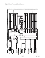
Страница 29: ...TEM CONTROL BLOCK DIAGRAM IIC BUS SDA 6dB AMP LPF DRIVER 5 VIDEO Pb Cb OUT VIDEO Y OUT VIDEO Pr Cr OUT JK2300 C2314 1 20 T M D S DATA2 T M D S DATA2 T M D S DATA1 T M D S DATA1 T M D S DATA0 T M D S DATA0 T M D S CLOCK T M D S CLOCK JK7501 HDMI CONNECTOR DDC DATA DDC CLOCK HOT PLUG DETECT IC7501 HDMI INTERFACE 6 4 9 7 10 12 3 1 15 19 16 REGISTER IIC I F VIDEO I F DDC I F AUTHENT CATION KEY EXCHANG...

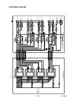
Страница 30: ...UTE L CH MUTE 16 14 15 IC7000 AUDIO D A CONVERTER AUDIO DAC 3 4 5 8 2 7 6 L CH R CH 1 R CH MUTE L CH MUTE 16 14 15 7 1 6 2 AUDIO L OUT AUDIO R OUT Q2203 MUTE ON Q2202 MUTE ON Q2200 DRIVE Q2201 DRIVE JK2200 IC2200 OP AMP 7 1 6 2 9 9 SURROUND L 7 7 SURROUND R 6 6 SURROUND MUTE 13 13 CENTER 11 11 SUB WOOFER 14 14 CENTER MUTE 10 10 SUB WOOFER MUTE 4 4 FRONT AUDIO L 2 2 FRONT AUDIO R 5 5 F AUDIO L MUTE...

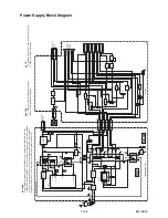
Страница 31: ...ERROR VOLTAGE DET 1 2 P ON 12V 1 P ON 10 5V SHUNT REG IC2601 IC2600 IC1005 D1001 D1004 BRIDGE RECTIFIER D1041 D1044 BRIDGE RECTIFIER DC DC CONVERTER SWITCHING CONTROL 5 2 3 5 AL 5V 1 AL 2 5V 6 AL 3 3V 20 F1 22 F2 23 FL 2 AL 12V 1 15 17 3 5 1 6 20 22 23 2 15 17 21 21 MAIN P ON AL 12V 2 CN1001 CN2600 11 AL 3 3V CN1002 FAN VCC 1 2 GND CN2004 SW 12V AUDIO 3 3V 1 3 P ON 10 5V 7 8 P ON 5V 1 CN2601 11 P ...

Страница 32: ... Do not use the part number shown on these drawings for ordering The correct part number is shown in the parts list and may be slightly different or amended since these drawings were prepared 2 To maintain original function and reliability of repaired units use only original replacement parts which are listed with their part numbers in the parts list section of the service manual 3 How to read con...

Страница 33: ...92 B 4 CN2003 F 1 R2021 C 2 R2094 B 4 CN2004 A 1 R2022 C 2 R2095 B 4 R2023 C 2 R2096 A 1 D2000 A 1 R2024 C 3 R2099 A 3 D2001 B 4 R2025 C 3 R2103 J 1 D2002 B 4 R2026 C 3 R2104 J 1 D2003 A 4 R2028 C 3 R2105 K 1 D2004 A 4 R2029 C 3 R2109 J 1 D2005 B 1 R2030 E 4 R2110 A 3 D2006 B 2 R2031 C 1 R2115 E 2 D2007 A 2 R2032 E 4 R2116 B 4 R2033 D 1 R2117 B 4 IC2000 D 2 R2034 D 3 R2118 B 4 IC2001 E 1 R2035 D 3...

Страница 34: ...AV1 1 11 3 SMD 3 5 0 2 5 PLAY mode STOP mode Voltage indications for PLAY and STOP modes on the Schematic Diagrams are as shown below 1 2 5 0 The same voltage for both PLAY STOP modes Indicates that the voltage is not consistent here ...

Страница 35: ...AV2 1 11 4 SMD 3 5 0 2 5 PLAY mode STOP mode Voltage indications for PLAY and STOP modes on the Schematic Diagrams are as shown below 1 2 5 0 The same voltage for both PLAY STOP modes Indicates that the voltage is not consistent here ...

Страница 36: ...2215 I 2 L2301 I 3 R2285 G 1 C2216 I 2 R2286 G 1 C2280 I 1 Q2100 J 2 R2287 G 1 C2281 I 1 Q2200 K 3 R2288 H 1 C2282 I 1 Q2201 J 2 R2308 I 4 C2283 I 1 Q2202 K 2 R2309 I 4 C2284 I 1 Q2203 K 2 R2310 K 4 C2285 H 1 Q2204 H 1 R2311 K 4 C2286 H 1 Q2205 H 1 R2312 K 4 C2287 I 1 Q2280 I 1 R2313 K 4 C2300 I 3 Q2300 H 3 R2323 H 3 C2301 I 3 Q2301 H 3 R2324 H 3 C2303 I 4 Q2302 H 1 R2328 J 3 C2304 I 3 R2330 H 1 C...

Страница 37: ...611 P 1 R2600 N 2 C2614 O 2 R2601 N 3 R2602 N 2 CN2600 M 4 R2603 N 3 CN2601 R 4 R2604 N 3 R2606 N 4 D2600 N 2 R2607 O 4 D2601 O 4 R2608 O 2 D2605 P 3 R2609 P 3 D2606 O 3 R2610 O 3 D2608 Q 4 R2612 N 2 D2609 Q 3 R2613 O 1 D2610 Q 3 R2615 O 1 D2611 Q 2 R2616 O 2 D2612 Q 2 R2617 O 2 D2613 N 3 R2619 O 1 D2614 O 2 R2620 P 2 R2621 O 2 IC2600 O 2 R2622 P 3 IC2601 O 1 R2623 P 2 R2626 Q 4 L2400 O 2 R2632 P ...

Страница 38: ...ram 1 11 7 SMD 3 5 0 2 5 PLAY mode STOP mode Voltage indications for PLAY and STOP modes on the Schematic Diagrams are as shown below 1 2 5 0 The same voltage for both PLAY STOP modes Indicates that the voltage is not consistent here ...

Страница 39: ... T 2 R2734 V 3 C2721 T 3 R2735 V 4 C2722 U 2 R2736 W 2 C2723 U 3 R2737 W 2 C2724 U 2 R2738 W 3 C2725 U 3 R2739 W 4 C2726 V 2 R2740 V 4 C2727 V 3 R2741 V 4 C2730 U 1 R2742 T 3 C2731 T 1 R2743 W 2 C2732 T 1 R2744 V 3 C2733 T 2 R2745 V 3 C2734 U 1 R2746 V 3 C2735 U 2 R2747 U 2 C2736 U 1 R2748 U 3 C2737 U 2 R2751 V 2 C2738 V 1 R2752 V 3 C2739 V 2 R2753 V 2 C2760 T 2 R2754 V 3 C2762 T 1 R2755 W 2 R2756...

Страница 40: ...AV CBA Top View BE5J10F01071A 1 11 9 ...

Страница 41: ...PIN 3 OF CN2000 PIN22OF CN2000 PIN 27 OF CN2000 WF6 WF4 WF8 WF7 WF1 WF5 WF2 WF4 PIN 5 OF CN2000 WF3 C2314 PLUS LEAD AV CBA Bottom View BE5J10F01071A 1 11 10 ...

Страница 42: ...E 5 R2012 B 1 C2315 A 5 C2738 C 4 L2280 B 3 R2014 A 2 COILS COILS CONNECTORS ICS TRANSISTORS RESISTORS CAPACITORS CAPACITORS DIODES CAPACITORS Ref No Position Ref No Position Ref No Position Ref No Position R2015 B 2 R2109 E 5 R2331 B 4 R2737 B 5 R2016 A 2 R2110 A 2 R2332 C 3 R2738 B 5 R2017 A 2 R2115 B 2 R2400 E 5 R2739 B 5 R2018 A 1 R2116 C 1 R2401 D 5 R2740 B 5 R2019 A 1 R2117 D 1 R2402 C 5 R27...

Страница 43: ... C1017 C 3 C1018 C 3 Q1003 B 1 C1019 C 2 Q1004 E 3 C1020 C 2 Q1012 D 3 C1021 C 2 C1022 D 2 R1002 B 2 C1023 D 3 R1003 B 2 C1024 D 3 R1004 B 2 C1025 D 2 R1005 A 1 C1026 E 4 R1006 B 2 C1040 C 4 R1008 B 2 C1041 B 4 R1009 B 2 C1042 B 4 R1011 B 1 C1043 B 4 R1012 B 1 C1044 C 3 R1013 B 2 C1045 B 3 R1014 C 1 C1046 C 4 R1016 C 1 C1047 D 4 R1017 C 1 C1048 C 3 R1018 C 2 C1049 D 4 R1019 D 1 C1051 E 4 R1020 D 1...

Страница 44: ...4 B 2 R1024 A 2 C1010 C 1 C1052 A 1 D1027 A 2 L1005 A 2 R1025 A 2 C1012 C 2 D1028 B 2 L1006 C 2 R1026 A 2 C1013 B 2 CN1001 A 2 D1031 B 2 L1007 A 2 R1030 A 1 C1014 A 2 CN1002 A 2 D1036 B 1 R1032 A 2 C1015 B 1 D1040 A 2 Q1003 B 1 R1034 A 1 C1016 B 2 D1001 C 2 D1041 C 2 Q1004 A 1 R1040 A 2 C1017 B 2 D1002 C 2 D1042 C 2 Q1012 A 2 R1041 A 1 C1018 B 2 D1003 C 2 D1043 C 2 R1046 B 2 C1019 A 1 D1004 C 2 D1...

Страница 45: ...CN3001 B 1 L3000 C 2 R3000 E 3 R3001 D 3 R3002 D 3 R3004 D 3 R3005 D 2 R3006 D 2 R3008 D 2 R3009 D 1 R3010 D 1 R3012 D 1 R3014 C 3 R3015 D 1 R3018 B 1 R3019 E 1 R3020 E 1 R3021 E 2 R3039 B 1 SW3000 D 1 SW3001 D 1 SW3002 D 1 SW3003 D 1 SW3004 E 1 SW3005 E 1 FL3000 C 3 RS3000 C 3 Front Schematic Diagram COIL RESISTORS MISCELLANEOUS CAPACITORS CONNECTORS SWITCHES ...

Страница 46: ... B 1 R3010 D 1 C3002 B 1 R3012 C 1 C3003 B 1 R3014 D 1 C3005 D 1 R3015 C 1 C3006 D 1 R3018 C 1 C3007 D 1 R3019 C 1 C3008 B 1 R3020 C 1 R3021 C 1 CN3000 C 1 R3039 A 1 CN3001 A 1 SW3000 D 1 L3000 D 1 SW3001 C 1 SW3002 C 1 R3000 C 1 SW3003 C 1 R3001 B 1 SW3004 C 1 R3002 B 1 SW3005 A 1 R3004 B 1 R3005 B 1 FL3000 B 1 R3006 B 1 RS3000 D 1 R3008 C 1 SWITCHES MISCELLANEOUS CAPACITORS CONNECTORS COIL RESIS...

Страница 47: ...16 BE5E10F01042 SD CBA Bottom View Ref No Position C4001 B 1 C4002 B 1 CN4001 C 2 CN4002 A 2 L4001 A 1 R4008 B 2 R4009 B 2 R4010 B 2 R4012 B 1 R4013 B 1 R4015 B 1 CAPACITORS CONNECTORS RESISTORS SD Schematic Diagram Parts Location Guide COIL ...

Страница 48: ... Diagram E5J10SCBM1 1 11 17 The order of pins shown in this diagram is different from that of actual IC6001 IC6001 is divided into eight and shown as IC6001 1 8 IC6001 8 8 in this BE Main Schematic Diagram Section 2 NOTE SMD ...

Страница 49: ...chematic Diagram E5J10SCBM2 The order of pins shown in this diagram is different from that of actual IC6001 IC6001 is divided into eight and shown as IC6001 1 8 IC6001 8 8 in this BE Main Schematic Diagram Section 2 NOTE SMD ...

Страница 50: ...chematic Diagram E5J10SCBM3 The order of pins shown in this diagram is different from that of actual IC6001 IC6001 is divided into eight and shown as IC6001 1 8 IC6001 8 8 in this BE Main Schematic Diagram Section 2 NOTE SMD ...

Страница 51: ... Diagram E5J10SCBM4 The order of pins shown in this diagram is different from that of actual IC6001 IC6001 is divided into eight and shown as IC6001 1 8 IC6001 8 8 in this BE Main Schematic Diagram Section 2 NOTE SMD 1 11 20 ...

Страница 52: ... Diagram E5J10SCBM5 The order of pins shown in this diagram is different from that of actual IC6001 IC6001 is divided into eight and shown as IC6001 1 8 IC6001 8 8 in this BE Main Schematic Diagram Section 2 NOTE SMD 1 11 21 ...

Страница 53: ... Diagram E5J10SCBM6 The order of pins shown in this diagram is different from that of actual IC6001 IC6001 is divided into eight and shown as IC6001 1 8 IC6001 8 8 in this BE Main Schematic Diagram Section 2 NOTE SMD 1 11 22 ...

Страница 54: ... Diagram E5J10SCBM7 The order of pins shown in this diagram is different from that of actual IC6001 IC6001 is divided into eight and shown as IC6001 1 8 IC6001 8 8 in this BE Main Schematic Diagram Section 2 NOTE SMD 1 11 23 ...

Страница 55: ... Diagram E5J10SCBM8 The order of pins shown in this diagram is different from that of actual IC6001 IC6001 is divided into eight and shown as IC6001 1 8 IC6001 8 8 in this BE Main Schematic Diagram Section 2 NOTE SMD 1 11 24 ...

Страница 56: ...BE Main 9 10 Schematic Diagram E5J10SCBM9 SMD 1 11 25 ...

Страница 57: ...BE Main 10 10 Schematic Diagram E5J10SCBM10 SMD 1 11 26 ...

Страница 58: ...BE Main CBA Top View 1 11 27 BE5E00G08016 ...

Страница 59: ...BE Main CBA Bottom View 1 11 28 BE5E00G08016 ...

Страница 60: ...ic Diagram E5J10SCFM1 The order of pins shown in this diagram is different from that of actual IC001 IC001 is divided into four and shown as IC001 1 4 IC001 4 4 in this FE Main Schematic Diagram Section 1 NOTE 1 11 29 SMD ...

Страница 61: ...ic Diagram E5J10SCFM2 1 11 30 The order of pins shown in this diagram is different from that of actual IC001 IC001 is divided into four and shown as IC001 1 4 IC001 4 4 in this FE Main Schematic Diagram Section 1 NOTE SMD ...

Страница 62: ...FE Main 3 5 Schematic Diagram E5J10SCFM3 1 11 31 SMD ...

Страница 63: ...ic Diagram E5J10SCFM4 1 11 32 The order of pins shown in this diagram is different from that of actual IC001 IC001 is divided into four and shown as IC001 1 4 IC001 4 4 in this FE Main Schematic Diagram Section 1 NOTE SMD ...

Страница 64: ...ic Diagram E5J10SCFM5 1 11 33 The order of pins shown in this diagram is different from that of actual IC001 IC001 is divided into four and shown as IC001 1 4 IC001 4 4 in this FE Main Schematic Diagram Section 1 NOTE SMD ...

Страница 65: ...CN2000 Pin 5 of CN2000 WF5 Pin 22 of CN2000 Pin 3 of CN2000 C2314 PLUS LEAD 20µs 0 5V VIDEO CVBS VIDEO Cr 0 2V 10µs VIDEO Cb 0 2V 10µs AUDIO L 1V 0 5ms SPDIF 1V 0 1µs NOTE Input Signal DVD VIDEO 75 COLOR BAR AUDIO 1KHz 0dB E5J10WF 1 12 1 ...

Страница 66: ... 15 16 17 18 STANDBY LED 18 CN2601 CN001 1 P ON 10 5V 2 P ON 10 5V 3 P ON 10 5V 4 GND 5 GND 6 GND 7 P ON 5V 1 8 P ON 5V 1 9 GND 10 GND 11 P ON 1 2V 12 GND 13 GND 14 P ON 3 3V 15 P ON 3 3V 1 2 3 4 5 6 7 8 9 10 11 12 13 14 15 CN2004 1 FAN VCC 2 GND 1 NSRST 2 GND 3 IDE1D7 4 IDE1D8 5 IDE1D6 6 IDE1D9 7 IDE1D5 8 IDE1D10 9 IDE1D4 10 IDE1D11 11 IDE1D3 12 IDE1D12 13 IDE1D2 14 IDE1D13 15 IDE1D1 16 IDE1D14 1...

Страница 67: ... the sequence it will stops and other sequence starts Only if SLED is moving it will stop after the moving is finished SLED position initialization Tray open SLED position initialization SLED inner around moves Tray Open Start Tray Close Start Tray Close End Tray Open End SLED moves Start Power on SLED moves End Hand close Hand close detection Start ...

Страница 68: ... Tray in sw Tray close retry off on off on Tray out sw Tray insertion direction Tray ejection direction T8 T3 t T1 Time out T6 Time out T7 If Tray out sw is not OFF within T7 it is Time out V1 V2 V0 0 Time out T4 Brake mode T5 Time out T11 Brake mode T9 t X V3 T3 If Tray out sw is not OFF within T6 it is Time out If Tray in sw is not ON within T11 it is Time out It raise up voltages until Tray in ...

Страница 69: ...2 30 NU Not Used 31 OUT AUDIO MUTE Audio Mute Control Signal 32 NU Not Used 33 OUT FL SDA FL Serial Data 34 OUT FL SCL FL Serial Clock 35 NU Not Used 36 NU Not Used 37 OUT PWSW3 Power On Signal Output 3 38 NU Not Used 39 OUT IIC BUS SDA IIC BUS Serial Data 40 OUT IIC BUS SCL IIC BUS Serial Clock 41 NU Not Used 42 OUT PWSW1 Power On Signal Output 1 43 IN RDY Ready Busy communication Control Signal ...

Страница 70: ...S E2 2SA1981Y AT 2SC1815 GR Y TE2 F T 2SC5343Y AT KTA1266 Y AT P KTA1271 Y AT P KTC3198 Y AT P STB1277LY AT STD1862LY AT 2SA1980M Y 2SC5343MG AT 2SC5343M Y KRA105M AT P KRC102M AT P KRC103M AT P KTA1267 Y AT P KTC3199 GR AT P KTC3205 Y AT P SRA2205M SRC1203MAT PQ070XF02SZH 2SK3798 Q PST3630NR PST8430NR EL817B LTV 817B F PS2561A 1 Q PS2561A 1 W FA5542N A2 TE1 TB7102F MM1636XWRE 2SA1530A T112 1Z 2SA...

Страница 71: ...1 RESET IC IC PST8430NR 1 C2016 ELECTROLYTIC CAP 47UF 6 3V M 1 C2016 CAP ELECTROLYTIC 47UF 6 3V M 1 C2018 ELECTROLYTIC CAP 47UF 6 3V M 1 C2018 CAP ELECTROLYTIC 47UF 6 3V M 1 C2019 CHIP RES 1608 1 10W 0 OHM 1 C2019 RES CHIP 1608 1 10W J 0 OHM 1 C2100 CHIP CERAMIC CAP 1608 B K 0 1UF 25V 1 C2104 ELECTROLYTIC CAP 47UF 6 3V M 1 C2104 CAP ELECTROLYTIC 47UF 6 3V M 1 C2106 CHIP CERAMIC CAP CH D 8PF 50V 1 ...

Страница 72: ...OLYTIC CAP 10UF 16V M 1 C2709 CAP ELECTROLYTIC 10UF 16V M 1 C2710 CHIP CERAMIC CAP CH J 220PF 50V 1 C2711 CHIP CERAMIC CAP CH J 220PF 50V 1 ELECTRICAL PARTS LIST BDP7200 12 Pos No 12 NC Description C2712 CHIP CERAMIC CAP CH J 39PF 50V 1 C2713 CHIP CERAMIC CAP CH J 39PF 50V 1 C2714 ELECTROLYTIC CAP 10UF 16V M 1 C2714 CAP ELECTROLYTIC 10UF 16V M 1 C2715 ELECTROLYTIC CAP 10UF 16V M 1 C2715 CAP ELECTR...

Страница 73: ...8 F0021 1 D2614 SWITCHING DIODE 1SS133 T 77 1 D2614 DIODE SWITCHING HSS4148TE E 1 ICS IC2000 IC SUB MICON MN101C77AFS3 1 If IC2001 is PST3630NR then C2013 is 0 1UF IC2001 RESET IC IC PST3630NR 1 ELECTRICAL PARTS LIST BDP7200 12 Pos No 12 NC Description C2013 CHIP CERAMIC CAP 1608 B K 0 1UF 25V 1 If IC2001 is PST8430NR then C2013 is 0 01UF IC2001 RESET IC IC PST8430NR 1 C2013 CHIP CERAMIC CAP B K 0...

Страница 74: ...1608 1 10W J 10K OHM 1 R2020 CHIP RES 1 10W J 10K OHM 1 R2020 RES CHIP 1608 1 10W J 10K OHM 1 R2021 CHIP RES 1 10W J 10K OHM 1 R2021 RES CHIP 1608 1 10W J 10K OHM 1 R2022 CHIP RES 1 10W J 10K OHM 1 R2022 RES CHIP 1608 1 10W J 10K OHM 1 R2023 CHIP RES 1 10W J 10K OHM 1 R2023 RES CHIP 1608 1 10W J 10K OHM 1 R2024 CHIP RES 1 10W J 100 OHM 1 R2024 RES CHIP 1608 1 10W J 100 OHM 1 R2025 CHIP RES 1 10W J...

Страница 75: ... OHM 1 R2215 CHIP RES 1 10W J 100K OHM 1 R2215 RES CHIP 1608 1 10W J 100K OHM 1 ELECTRICAL PARTS LIST BDP7200 12 Pos No 12 NC Description R2216 CHIP RES 1 10W J 220 OHM 1 R2216 RES CHIP 1608 1 10W J 220 OHM 1 R2217 CHIP RES 1 10W J 1K OHM 1 R2217 RES CHIP 1608 1 10W J 1 0K OHM 1 R2218 CHIP RES 1 10W J 220 OHM 1 R2218 RES CHIP 1608 1 10W J 220 OHM 1 R2219 CHIP RES 1 10W J 1K OHM 1 R2219 RES CHIP 16...

Страница 76: ...CHIP RES 1 10W J 4 7K OHM 1 ELECTRICAL PARTS LIST BDP7200 12 Pos No 12 NC Description R2716 RES CHIP 1608 1 10W J 4 7K OHM 1 R2717 CHIP RES 1 10W J 2 2K OHM 1 R2717 RES CHIP 1608 1 10W J 2 2K OHM 1 R2720 CHIP RES 1 10W F 8 2K OHM 1 R2720 CHIP RES 1608 1 10W F 8 2K OHM 1 R2720 RES CHIP 1608 1 10W F 8 20K OHM 1 R2721 CHIP RES 1 10W J 12K OHM 1 R2721 RES CHIP 1608 1 10W J 12K OHM 1 R2722 CHIP RES 1 1...

Страница 77: ... B K 1000PF 50V 1 C3006 CHIP CERAMIC CAP 1608 F Z 0 1UF 50V 1 ELECTRICAL PARTS LIST BDP7200 12 Pos No 12 NC Description C3007 ELECTROLYTIC CAP 100UF 6 3V M H7 1 C3008 CHIP CERAMIC CAP 1608 B K 0 1UF 25V 1 CONNECTORS CN3000 WX1E5E10 003 18 155 1 0 1 CN3001 CONNECTOR PRINT OSU S3B PH K S LF SN 1 COIL L3000 INDUCTOR 100UH K LAP02TA101K 1 RESISTORS R3000 CHIP RES 1 10W J 10 OHM 1 R3000 RES CHIP 1608 1...

Страница 78: ...C CAP 2200UF 25V M 1 C1025 ELECTRIC CAP 4700UF 10V 1 C1025 CAP ELECTROLYTIC 4700UF 10V M 1 C1025 ELECTROLYTIC CAP 4700UF 10V M 1 ELECTRICAL PARTS LIST BDP7200 12 Pos No 12 NC Description C1026 CHIP CERAMIC CAP 1608 F Z 0 1UF 50V 1 C1040 SAFETY CAP 2200PF 250V 1 C1040 SAFETY CAP 2200PF 250V 1 C1041 ELECTROLYTIC CAP 10UF 400V M 1 C1041 CAP ELECTROLYTIC 10UF 400V M 1 C1042 METALIZED FILM CAP 0 0022UF...

Страница 79: ...7 1 D1048 DIODE SWITCHING HSS4148TE E 1 D1049 DIODE SWITCHING 1N4148 F0021 1 D1049 SWITCHING DIODE 1SS133 T 77 1 D1049 DIODE SWITCHING HSS4148TE E 1 ELECTRICAL PARTS LIST BDP7200 12 Pos No 12 NC Description D1050 DIODE ZENER 27BSB T26 1 D1050 ZENER DIODE MTZJT 7727B 1 D1052 DIODE SWITCHING 1N4148 F0021 1 D1052 SWITCHING DIODE 1SS133 T 77 1 D1052 DIODE SWITCHING HSS4148TE E 1 D1053 DIODE ZENER 27BS...

Страница 80: ...HM 1 R1054 CHIP RES 1 10W J 470K OHM 1 R1054 RES CHIP 1608 1 10W J 470K OHM 1 R1055 CHIP RES 1 10W J 33K OHM 1 R1055 RES CHIP 1608 1 10W J 33K OHM 1 R1056 CHIP RES 1 10W J 470 OHM 1 R1056 RES CHIP 1608 1 10W J 470 OHM 1 R1057 CHIP RES 1 10W J 3 3K OHM 1 R1057 RES CHIP 1608 1 10W J 3 3K OHM 1 R1058 CHIP RES 1 10W J 4 7K OHM 1 R1058 RES CHIP 1608 1 10W J 4 7K OHM 1 R1060 CHIP RES 1608 1 10W 0 OHM 1 ...

Страница 81: ... 2L027 B49 A3 A4 B5 A2 B12 A6 B15 AV CBA 2L044 2L050 2L034 B14 B14 W01 2L085 B53 B54 2L085 A8 A21 2L037 B4 2L026 2L026 B34 B38 2L034 2L034 2L034 2L034 2L081 2L083 2L070 2L070 A24 SD01 FM01 W08 A11 A1X A10 B13 A20 2L018 W11 W09 POWER SUPPLY CBA BE MAIN CBA Unit SD CBA POWER SW CBA FRONT CBA FE MAIN CBA BD Mechanism Assembly B52 W07 W06 W05 W04 B47 2L056 2L055 F1001 ASSY 4 ASSY 3a ASSY 2 ASSY 5 ASSY...

Страница 82: ...1 18 2 E5J10PEX Packing Unit S2 A20 S3 S1 S1 X10 X19 X24 X38 X3 X15 X14 X6 X10 Lower Side Upper Side Lower Side Upper Side X2 A B C D E F G H I X1 A B C Some Ref Numbers are not in sequence A35 ...

Страница 83: ... PCB HOLDER ASSEMBLY E5H40UD 1 B13 FRONT BRAKET R E5E10UD 1 B14 996510010148 LOCKING CARD SPACER KGLS 22S 1 B15 SD CARD HOLDER E5E10UD 1 B34 DOUBLE SIDE TAPE E5E10UD 1 B38 996510012103 CORE FERRITE HF70SH25 0 7 10 1 B52 996510012104 CUSHIION E5E10UD 1 B53 996510012105 CONDUCTIVE TAPE CSTK 026065 1 B54 996510012106 CONDUCTIVE TAPE CSTK 040055 1 FM01 996510018695 MOTOR DC FAN 2D65BL100120 1 SD01 996...

Отзывы: