


EN 36
3139 785 32970
5.
Fireware Upgrading
5.2. Procedure to reset the settings to initial mode
1. Power up the set without any disc inserted.
2. When the set displays: “HOME MENU”, press and hold the skip forward key on the Front Panel of the set as shown in figure 1.
Figure 1
3. The initial mode will be activated and the set will display:
“NO DISC”
4. On the TV Screen, it will show the language selection menu as shown in figure 2 and select the Language by pressing the
corresponding key as described in the menu.
Figure 2
Note: Resetting the initial mode will restore all the user settings to Default.
Содержание BDP7100/12
Страница 3: ...EN 3 3139 785 32970 1 Location PCB Drawing MAIN PCB S M P S PCB BDP LOADER ASSY 1 11 PCB Location ...
Страница 37: ...EN 37 3139 785 32970 6 Block and Wiring Diagram 6 1 All block Diagram ...
Страница 38: ...EN 38 3139 785 32970 6 Block and Wiring Diagram 6 2 Wiring Diagram ...
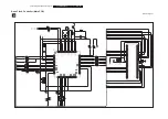
Страница 40: ...EN 40 3139 785 32970 7 Circuit Diagrams and PCB Layouts SMP8634 DDR SDRAM Main PCB Schematic Diagrams 2 ...
Страница 41: ...EN 41 3139 785 32970 7 Circuit Diagrams and PCB Layouts SMP8634 Flash Memory Main PCB Schematic Diagrams 3 ...
Страница 42: ...EN 42 3139 785 32970 7 Circuit Diagrams and PCB Layouts Schematic Diagrams Nand Flash Controller Main PCB 4 ...
Страница 43: ...EN 43 3139 785 32970 7 Circuit Diagrams and PCB Layouts SMP8634 Power Decoupling Main PCB Schematic Diagrams 5 ...
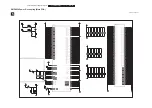
Страница 45: ...EN 45 3139 785 32970 7 Circuit Diagrams and PCB Layouts HDMI CEC Main PCB Schematic Diagrams 7 ...
Страница 46: ...EN 46 3139 785 32970 7 Circuit Diagrams and PCB Layouts Ethernet contol Main PCB Schematic Diagrams 8 ...
Страница 51: ...EN 51 3139 785 32970 7 Circuit Diagrams and PCB Layouts Power Main PCB Schematic Diagrams 13 ...
Страница 52: ...EN 52 3139 785 32970 7 Circuit Diagrams and PCB Layouts PCI ETC Main PCB Schematic Diagrams 14 ...
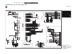
Страница 53: ...EN 53 3139 785 32970 7 Circuit Diagrams and PCB Layouts Front Interface Main PCB Schematic Diagrams Power 15 ...
Страница 55: ...EN 55 3139 785 32970 7 Circuit Diagrams and PCB Layouts Power Key Power Key PCB Schematic Diagrams 17 ...
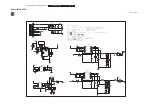
Страница 60: ...EN 60 3139 785 32970 7 Circuit Diagrams and PCB Layouts PCB Diagrams CONDUCTOR SIDE Layout S M P S PCB ...


