


EN 33
3139 785 32970
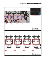
4.
Trouble Shooting
NO LOGO (CVBS, S-Video)
Video
selection
accords with cable connection
and TV mode?
Video
output from
MIC1 (VC2, VC3,VC4)
Video
output from
VIC1?(VR7,VR21,VR22)
Component cable error
Check the Video select, cable
connection, TV mode
MIC1 soldering error
Check VIC1 soldering of
peripheral devices
No
Yes
No
No
Yes
Yes
Refer to Fig. 4-10
Refer to Fig. 4-10
Содержание BDP7100/12
Страница 3: ...EN 3 3139 785 32970 1 Location PCB Drawing MAIN PCB S M P S PCB BDP LOADER ASSY 1 11 PCB Location ...
Страница 37: ...EN 37 3139 785 32970 6 Block and Wiring Diagram 6 1 All block Diagram ...
Страница 38: ...EN 38 3139 785 32970 6 Block and Wiring Diagram 6 2 Wiring Diagram ...
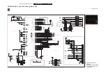
Страница 40: ...EN 40 3139 785 32970 7 Circuit Diagrams and PCB Layouts SMP8634 DDR SDRAM Main PCB Schematic Diagrams 2 ...
Страница 41: ...EN 41 3139 785 32970 7 Circuit Diagrams and PCB Layouts SMP8634 Flash Memory Main PCB Schematic Diagrams 3 ...
Страница 42: ...EN 42 3139 785 32970 7 Circuit Diagrams and PCB Layouts Schematic Diagrams Nand Flash Controller Main PCB 4 ...
Страница 43: ...EN 43 3139 785 32970 7 Circuit Diagrams and PCB Layouts SMP8634 Power Decoupling Main PCB Schematic Diagrams 5 ...
Страница 45: ...EN 45 3139 785 32970 7 Circuit Diagrams and PCB Layouts HDMI CEC Main PCB Schematic Diagrams 7 ...
Страница 46: ...EN 46 3139 785 32970 7 Circuit Diagrams and PCB Layouts Ethernet contol Main PCB Schematic Diagrams 8 ...
Страница 51: ...EN 51 3139 785 32970 7 Circuit Diagrams and PCB Layouts Power Main PCB Schematic Diagrams 13 ...
Страница 52: ...EN 52 3139 785 32970 7 Circuit Diagrams and PCB Layouts PCI ETC Main PCB Schematic Diagrams 14 ...
Страница 53: ...EN 53 3139 785 32970 7 Circuit Diagrams and PCB Layouts Front Interface Main PCB Schematic Diagrams Power 15 ...
Страница 55: ...EN 55 3139 785 32970 7 Circuit Diagrams and PCB Layouts Power Key Power Key PCB Schematic Diagrams 17 ...
Страница 60: ...EN 60 3139 785 32970 7 Circuit Diagrams and PCB Layouts PCB Diagrams CONDUCTOR SIDE Layout S M P S PCB ...


