F3SG-RA
2
5
NPN Output
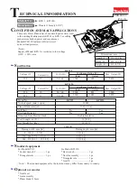
Input Circuit Diagram by Function
The input circuit diagrams of by function are shown below.
PNP Output
NPN Output
2
1
5
8
7
6
+24 VDC
1
2
4
Bro
w
n
Black TEST
White
N
ot
u
sed
Bl
u
e
Bro
w
n
Yello
w
White OSSD 2
Pink MUTE B
Gray MUTE A
Black OSSD 1
Red AUX
Bl
u
e
3
Reset inp
u
t
circ
u
it
4
M
u
ting inp
u
t
circ
u
it B
3
M
u
ting inp
u
t
circ
u
it A
RESET
0 VDC
5
Yello
w
N
ot
u
sed
Indicator
Emitter
Main Circ
u
it
Test Inp
u
t
Circ
u
it
Recei
v
er
Main Circ
u
it 2
Recei
v
er
Main Circ
u
it 1
Indicator
Load
Load
Load
Emitter
Main
Circuit
+24 VDC
0 VDC
5 V
Short circuit current:
3 mA
<Input circuit (Test input)>
Receiver
Main
Circuit
+24 VDC
0 VDC
Short circuit current *
<Input circuit (Reset input, Muting inputs A/B)>
Receiver
Main
Circuit
+24 VDC
0 VDC
Short circuit current *
<Input circuit (Reset, Muting inputs A/B)>
Emitter
Main
Circuit
+24 VDC
0 VDC
5 V
Short circuit current:
3 mA
<Input circuit (Test input)>
*Short circuit current: 5mA (Reset input), 3mA (Muting inputs A/B)