


UM10525
All information provided in this document is subject to legal disclaimers.
© NXP B.V. 2012. All rights reserved.
User manual
Rev. 1 — 19 April 2012
16 of 21
NXP Semiconductors
UM10525
120 V 20 W CFL demo board using the UBA2212
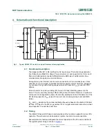
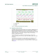
6. Schematic and Bill Of Materials (BOM)
The components used are illustrated in
Figure 3
and
Figure 13
.
Table 3
describes the components required for 120 V reference board application.
Fig 13. Application diagram
001aan371
Rfuse
D3
CBUF
C5
C8
C7
C6
L2
RCSI
CDVDT
Cosc
CCB
CVDD
Rosc
CSW
CFS
LFILT
D2
D4
D1
U1
OUT
1
14
FS
SGND
2
13
SGND
HV
3
12
SENSE
PGND
4
11
SGND
DVDT
5
10
CSI
V
DD
6
9
CB
RC
7
8
SW
CFL
AC input
L_N
L_L
UBA2212
Table 3.
Bill of materials
Number Reference
Typical value
Quantity
1
R
fuse
10
; 1 W - no value for fuse resistor
1
2
D1, D2, D3, D4
diode, 1 A; 1000 V; 1N4007
4
3
C
BUF
electrolytic capacitor; 33
F; 250 V; 105
C
1
4
L
FILT
inductor; 3 mH; 0.5 A
1
5
C
DVDT
ceramic capacitor; 330 pF; 500 V; 1206
1
6
C
FS
ceramic capacitor; 22 nF; 50 V; 0805
1
7
C
CB
ceramic capacitor; 220 nF; 50 V; 0805
1
8
C
SW
ceramic capacitor; 68 nF; 50 V; 0805
1
9
C
osc
ceramic capacitor; 220 pF; 50 V; 0805
1
10
C
VDD
ceramic capacitor; 100 nF; 50 V; 0805
1
11
R
osc
chip resistor; 100 k
; 5 %; 0805
1
12
C6; C7
film capacitor; 82 nF; 100 V
2
13
C5
film capacitor; 6.8 nF; 1 kV
1
14
C8
film capacitor; 8.2 nF; 400 V
1
15
R
CSI
chip resistor; 1.8
; 1 %; 0.25 W
1