


UM10525
All information provided in this document is subject to legal disclaimers.
© NXP B.V. 2012. All rights reserved.
User manual
Rev. 1 — 19 April 2012
12 of 21
NXP Semiconductors
UM10525
120 V 20 W CFL demo board using the UBA2212
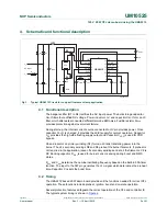
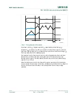
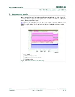
5.2 RMS control in boost and steady states
When ignition frequency is reached, the lamp ignites. V
SW
increases to a given voltage to
set the lamp current at the level defined by the internal boost reference and resistor R
CSI
.
The calculation is shown in
Equation 1
:
(1)
When the RMS current control circuit leaves the system operating at the normal lamp
current, it enters the steady state. In this state, the voltage on pin CB is fixed and a
feedback loop controls the voltage on pin SW. This feature enables the lamp current to be
independent of the mains or lamp voltage. The lamp current calculation is shown in
Equation 2
:
(2)
Therefore, the boost-burn ratio can be found as shown in
Equation 3
:
(3)
5.3 Overtemperature
protection
OTP is active in all states except boost. When the die temperature reaches the OTP
activation threshold (T
th(act)otp
), the oscillator is stopped and the power switches
(LSPT/HSPT) are set to the start-up state. When the oscillator is stopped, the DVDT
supply no longer generates the supply current I
DVDT
. Voltage V
DD
gradually decreases
and the start-up state is entered. OTP is reset when the temperature < T
th(rel)otp
.
During boost state, the threshold of temperature is T
j(end)bst
which is lower than T
th(otp)
.
When the die temperature has reached T
j(end)bst
, the boost state ends, the IC enters
steady state and OTP is enabled.
Boost I
lamp
V
ref bst
R
CSI
-------------------
=
Burn I
lamp
V
ref burn
R
CSI
-----------------------
=
Boost to burn ratio
V
ref bst
V
ref burn
-----------------------
=