


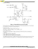


3.10.2 Resolver Generator Output
The RES_GEN source signal is output from TIM0 timer module, PT0. The output signal level is set up by trimmer R78.
Figure 23. Resolver output interface
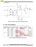
3.11 User Interface
Several general-purpose features are available on board, and are configurable by the user for different applications.
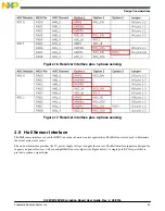
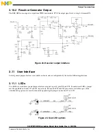
3.11.1 LEDs
Two LEDs are available as general purpose features, mapped to port S, pins PS4 and PS5. To enable each LED, a jumper
must be populated on header J37 and J53, respectively. Because the PS4 and PS5 pins are also available as part of the
extended debug option, care must be taken when populating the jumpers on headers J37 and J53.
Figure 24. User LED options
Design Considerations
S12ZVM12EVB Evaluation Board User Guide, Rev. 2, 03/2016
Freescale Semiconductor, Inc.
27