


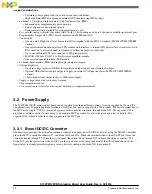


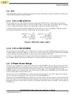

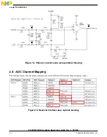


Figure 3. Boost DC/DC converter option
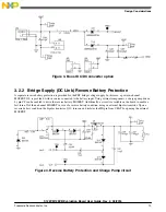
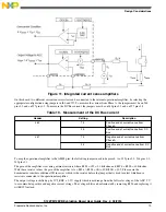
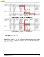
3.2.2 Bridge Supply (DC Link) Reverse Battery Protection
A separate reverse battery protection is provided for the FET bridge voltage supply. In this case, a power n-channel
MOSFET, Q9, is provided, with its source connected to the battery input. Using external components, a charge pump driven
by pin CP can be enabled to drive the reverse battery MOSFET. Additionally, a circuit is available on the board to enable a
fast turn-off of the n-channel MOSFET in case of a reverse battery condition, using an external bipolar transistor. Upon a
reverse battery condition, the bipolar transistor, Q10, turns on and isolates the HD pin from VBAT by opening the external
MOSFET.
Figure 4. Reverse Battery Protection and Charge Pump circuit
Design Considerations
S12ZVM12EVB Evaluation Board User Guide, Rev. 2, 03/2016
Freescale Semiconductor, Inc.
13