


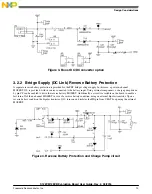


3.5 SCI
The S12ZVM EVB provides two different routing options to link one SCI module on the microcontroller to a USB port that
could be easily connected to a personal computer.
3.5.1 SCI to USB (CP2102)
The first alternative is to use the USB interface that is provided with the CP2102 USB to UART bridge. This interface is
available through a Type B USB connector, J25, and is digitally isolated. A driver needs to be installed on the host computer
to create a virtual serial COM port, linked to the USB port that is connected to the USB to UART bridge.
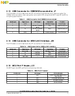
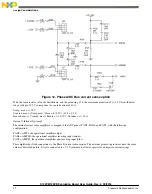
A couple of jumpers need to be populated on headers J27 and J28 from pin 2 to pin 3 on both headers. This links the SCI1
pins from the microcontroller to the USB to UART bridge, through the digital isolator.
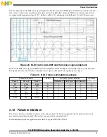
Figure 9. USB to SCI jumper options
3.5.2 SCI to USB (OSBDM)
The second option to route the SCI1 port to a USB interface is by using the on-board OSBDM programmer. This interface is
available through a Type B USB connector, J7. The necessary drivers to operate the serial interface provided by the OSBDM
device should install the first time the EVB is connected to the computer through a USB cable.
In this case, a couple of jumpers need to be placed on headers J27 and J28 from pin 1 to pin 2 on both headers. This will
route the RXD and TXD signals from the SCI1 module, to the RXD and TXD signals from the OSBDM device.
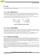
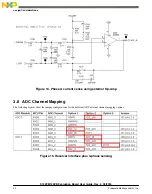
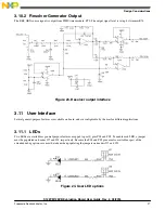
3.6 3-Phase Power Bridge
The power stage is configured as a 3-phase Power Bridge with n-channel MOSFET transistors. The Gate Driver Unit (GDU)
integrated into the MCU provides the supply voltage to the gates of the low-side and high-side MOSFETs. The GDU pins are
designed to interface to external components in the automotive battery range, so they can be connected directly to the
MOSFET terminals. For evaluation purposes, the connections from the GDU pins to the MOSFETs on the S12ZVM128EVB
board are done through a series of 0-ohm resistors.
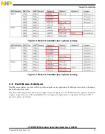
The drivers for the low-side MOSFET gates are driven by the internal LDO regulator (VLS_OUT). Each driver uses the pin
LSx as its reference, and supplies the voltage into pin LGx to drive the MOSFET gate.
The drivers for the high-side MOSFET gates are driven by the voltage stored in a bootstrap capacitor, which is external to the
MCU. This voltage is derived from the LDO regulator through an external diode and fed into the bootstrap voltage VBSx pin.
Each high-side driver uses the pin HSx as its reference, and supplies the bootstrap voltage into pin HGx to drive the high-side
MOSFET gate.
Design Considerations
S12ZVM12EVB Evaluation Board User Guide, Rev. 2, 03/2016
Freescale Semiconductor, Inc.
17