


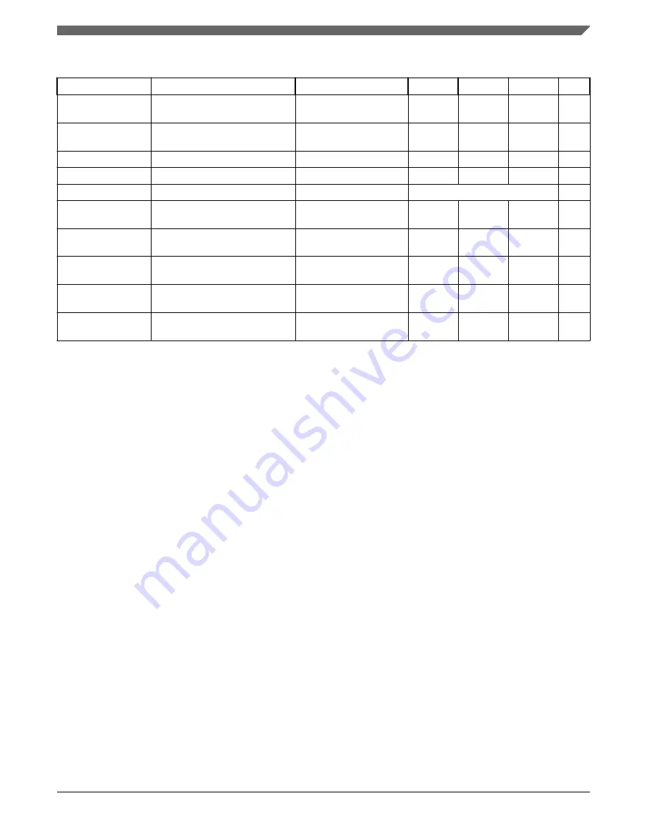
Table 19. ADC conversion characteristics (continued)
Symbol
Parameter
Conditions
Min
Typ
Max
Unit
SNR
Signal-to-noise ratio
V
REF
= 3.3 V, Fin ≤ 125
kHz
66
—
—
dB
SNR
Signal-to-noise ratio
V
REF
= 5.0 V, Fin ≤ 125
kHz
68
—
—
dB
THD
Total harmonic distortion
@ 125 kHz
65
70
—
dB
Effective number of bits
Fin < 125 kHz
10.5
—
—
bits
SINAD
Signal-to-noise and distortion
Fin < 125 kHz
(6.02*ENOB)+1.76
dB
TUE
IS1WINJ
Total unadjusted error for
IS1WINJ
Without current injection
–6
—
6
LSB
TUE
IS1WWINJ
Total unadjusted error for
IS1WWINJ
Without current injection
–6
—
6
LSB
I
DD_VDDA
Maximum operating current on
VDDA
Tj = 150C VDD_LV_COR
= 1.32 V
—
3.7
5
mA
I
DD_VDDR
Maximum operating current on
VREF
Tj = 150C VDD_LV_COR
= 1.32 V
—
150
600
μA
V
BG_REF
Band gap reference for self test
Trimmed,
INPSAMP=0xFF
1.164
—
1.236
V
1. V
DD_HV_IO
= 3.3 V -5%,+10%, T
J
= –40 to +150 °C, unless otherwise specified, and analog input voltage from V
AGND
to
V
AREF
2. SAR ADC performance is not guaranteed when IRC is used as clock source for PLL0 to generate SAR ADC clock.
3. AD_CK clock is always half of the ADC module input clock defined via the auxiliary clock divider for the ADC.
4. During the sample time the input capacitance C
S
can be charged/discharged by the external source. The internal
resistance of the analog source must allow the capacitance to reach its final voltage level within t
sample
. After the end of the
sample time t
sample
, changes of the analog input voltage have no effect on the conversion result. Values for the sample
clock t
sample
depend on programming.
5. This parameter does not include the sample time t
sample
, but only the time for determining the digital result and the time to
load the result register with the conversion result.
6. See the above figure.
7. Subject to change with additional -40°C characterization on final silicon version.
8. Below 4.5V, ENOB - 9.5b, THD- 60dB at Fin= 125KHz
9. Band gap reference only applies to Cut 2 silicon.
10. Minimum and maximum values are t/-3%
NOTE
• For spec complaint operation, do not expose clock sources,
including crystal oscillator, IRC, PLL0, and PLL1 on the
CLKOUT pads while the SAR ADC is converting.
• The ADC performance specifications are not guaranteed if
two or more ADCs simultaneously sample the same shared
channel.
11.3 S/D ADC
The SD ADCs are Sigma Delta 16-bit analog-to-digital converters with 333 Ksps
maximum output rate.
ADC modules
SPC5746R Microcontroller Data Sheet, Rev. 6, 06/2017
NXP Semiconductors
29


