


6. This LVD/HVD disabled supply voltage condition only applies after LVD/HVD are disabled by the application during the
reset sequence, and the LVD/HVD are active until that point.
7. The pad are operative till 3.0V full performance. The IRC oscillator is supplied by this pin and it is setting the min voltage
limit.
8. FEC will be used only in 3.3V mode. In 5V mode the segment is a general IO segment with the same characteristics of
IO_MAIN.
9. MSC will be used only in 3.3V mode. In 5V mode the segment is a general IO segment with the same characteristics of
IO_MAIN.
10. If XOSC is enabled via DCF_UTEST_Miscellaneous[XOSC_EN], V
DD_HV_IO_JTAG
must be within the operating range
before RESET pin is released.
11. JTAG will be used only in 3.3V mode. In 5V mode the segment is a general IO segment with the same characteristics of
IO_MAIN.
12. The startup of flash regulator and memory initialization immediately after Phase0 of reset sequence could cause a drop of
the PMC supply. No LVD event will be generated as during this time the LVD monitors are not enabled.
13. V
DDSTBY
supply must be present before and after power up/down of the device supplies and the ramp rate should be less
than 33.3 kV/s.
14. RAM retention is not guaranteed below 1.3 V, but no effect on RAM operation for voltages below 1.3 V when V
DD_LV
is
above the minimum value.
15. For supply voltages between 3.6V and 4.5V there will be no guaranteed precision of ADC (accuracy/linearity). ADC will
recover to a fully functional state when the voltage rises above 4.5V.
16. V
DD_HV_ADV_SD
must be higher or equal than the V
DD_HV_ADV_SAR
supply to guarantee full performance. It is recommended
to connect the V
DD_HV_ADV_SD
to V
DD_HV_ADV_SAR
at board level.
17. Temperature Sensor and its associated Band-Gap reference are supplied by this pin. The temperature sensor
performance is guaranteed only between 4.5 V and 5.5 V.
18. Full device lifetime without performance degradation.
19. I/O and analog input specifications are only valid if the injection current on adjacent pins is within these limits. See the
absolute maximum ratings table for maximum input current for reliability requirements.
20. The I/O pins on the device are clamped to the I/O supply rails for ESD protection. When the voltage of the input pin is
above the supply rail, current will be injected through the clamp diode to the supply rail. For external RC network
calculation, assume typical 0.3 V drop across the active diode. The diode voltage drop varies with temperature. For more
information, see the device characterization report.
21. Sum of all controller pins (including both digital and analog) must not exceed 200 mA. A V
DD_HV_IO
power segment is
defined as one or more GPIO pins located between two V
DD_HV_IO
supply pins.
22. The average current values given in the "I/O pad current specifications" section should be used to calculate total I/O
segment current.
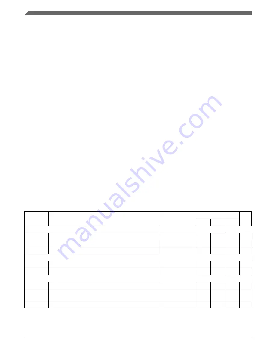
Table 4. Emulation (buddy) device operating conditions
Symbol
Parameter
Conditions
Value
Unit
Min
Typ
Max
Frequency
—
Standard JTAG 1149.1/1149.7 frequency
—
—
—
50
MHz
—
High-speed debug frequency
—
—
—
320
MHz
—
Data trace frequency
—
—
—
1250 MHz
Temperature
T
J_BD
Device junction operating temperature range
Packaged devices –40.0
—
150.0
°C
T
A _BD
Ambient operating temperature range
Packaged devices –40.0
—
125.0
°C
Voltage
V
DD_LV_BD
Buddy core supply voltage
—
1.18
—
1.32
V
V
DD_HV_IO_B
D
Buddy I/O supply voltage
—
3.0
—
5.5
V
V
RAMP_BD
Buddy slew rate on power supply pins
—
—
—
500
V/ms
Operating conditions
SPC5746R Microcontroller Data Sheet, Rev. 6, 06/2017
10
NXP Semiconductors


