


When touch happens, input capacitance C
x
increases. The charging current of C
i
becomes larger and then the number of V
ci
ramp
up steps is reduced. The output count of digital SINC filter is reduced, so the value of
TSIx_DATA[TSICNT]
is decreased.
2.2.2 Noise cancellation mode of self-cap
If touch sensor encounters strong low frequency noise, noise cancellation can be activated by setting
TSIx_MODE[S_NOISE]
.
In the noise cancellation mode, vdd3v, and vddlv (1.2 V) are dual sample voltages. Two phases exist in noise
cancellation architecture:
• Charging phase of C
i
when vdd3v is on and vddlv is off
• Discharging phase of C
i
when vdd3v is off and vddlv is on
Two switching clock cycles are cost to samples twice which includes charging phase (sampling vdd3v) and discharging phase
(sampling vddlv). The input current of C
i
equal to charging phase current abstract discharging phase current. At the end of each
second phase, low frequency noise is subtracted. In a long integration period, the noise induced error can be canceled.
2.2.3 Sensitivity boost mode of self-cap
The larger parasitic capacitance causes the low sensitivity. The low sensitivity results in the difficulty to recognize the touch event.
For example, when the touch overlay is very thick, it becomes very hard to detect a touch event correctly.
To increase the sensitivity, enable sensitivity-boost feature by removing part parasitic capacitance virtually. So touch works well
under the thicker overlay with sensitivity boost enabled.
The capacitance to be removed cannot be configured more than the intrinsic capacitance of the touch key.
Otherwise, it causes the sensitivity invalid.
NOTE
2.3 Clock generation
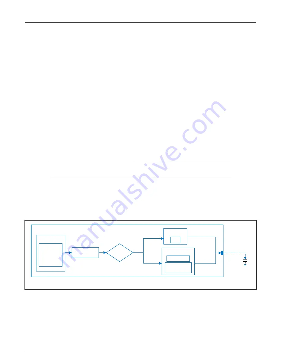
The clock generation determines the TSI scan speed. The maximum frequency of TSI is about 10 MHz.
The TSI module is only clocked by the main clock, which is generated by TSI module itself without any other external clock source.
The main clock has four ranges of frequency. It can be divided into the switching clock which is used to control the ph1/ph2
switching speed and finally determines the whole scan time, as shown in
.
SSC
Main Clock
20.72MHz
16.65MHz
13.87MHz
11.91MHz
SSC_MODE
PRBS SSC
No SSC
Up
-
down
counter SSC
Touch Key
Switching Clock
SSC_MODE = 10b
SSC_MODE = 00b/
01
b
basic
advanced
1/ 2
Main Clock
Pr 1
Figure 9. Block diagram of clock generation
• When SSC_MODE = 10b, the switching clock is divided from main clock directly, as the basic clock generation.
• When SSC_MODE = 00b/01b, the switching clock is generated from SSC module, as the advanced clock generation.
2.3.1 Basic clock generation
si the basic clock generation, when TSIx_SSC0[SSC_MODE] = 10b.
NXP Semiconductors
TSI self-cap mode introduction
KE17Z Dual TSI User Guide, Rev. 0, 05 May 2022
User Guide
9 / 37