


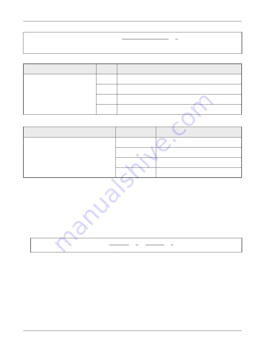
Switcℎing Clock =
Main Clock
SSC_PRESCALE_NUM + 1 ×
1
2
Equation 1.
Table 4. Main clock setting
Register
Value
Main clock (MHz)
TSI_MODE[SETCLK]
00
20.72
01
16.65
10
13.87
11
11.91
Table 5. Divider setting
Register
Value
SSC_PRESCA 1
TSI_SSC0.SSC_PRESCALE_NUM[7:0]
00000000
divide 1
00000001
divide 2
…
…
11111111
divide 256
There is an example of the basic clock generation, the main clock as 16.65 MHz, the divider as 16, and the result of switching clock
is 1.04 MHz.
To use no SSC switching clock with frequency of 1 MHz,
• Set SETCLK < 1:0 > to ‘01b’ to get main clock = 16.65 MHz.
• Set SSC_MODE < 1:0 > to ‘10b’ to disable SSC function.
• Set SSC_PRESCALE_NUM < 7:0 > to ‘00000111b’ to get division 8. When SSC mode is disabled, the frequency is
main
clock/[(SSC_PRESC1) × 2]
.
• Keep other registers in TSIx_SSC0, TSIx_SSC1, and TSIx_SSC2 as default value.
Switcℎing Clock = Main Clock
Divider ×
1
2 =
16.65 MHz
8
× 12 = 1.04 MHz
2.3.2 Advanced clock generation, spread spectrum clocking
The Spread Spectrum Clocking (SSC) increases the noise immunity to RF interference and spreads the emissions.
With the SSC enabled (TSIx_SSC0[SSC_MODE] = 00/01b), the switching clock is generated by the SSC module, other than the
direct divided main clock.
In the Self-cap mode, changing the SSC charge time does not affect the final scan result. It changes the total scan time as it
changes the switching clock frequency.
If SSC mode is enabled, the timing of the switching clock generation is as shown in
.
NXP Semiconductors
TSI self-cap mode introduction
KE17Z Dual TSI User Guide, Rev. 0, 05 May 2022
User Guide
10 / 37