


NXP Semiconductors
FS4500/FS6500 evaluation boards
KTFRDMFS4500-FS6500EVMUG
FS4500/FS6500 evaluation boards
All information provided in this document is subject to legal disclaimers.
© NXP B.V. 2017. All rights reserved.
User guide
Rev. 4.0 — 12 June 2017
17 / 34
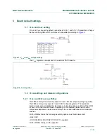
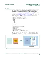
5 Board default settings
5.1 V
CCA
and V
AUX
setting
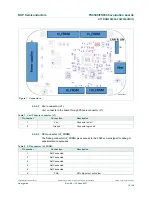
V
CCA
and V
AUX
are set by default, respectively to 3.3 V and 5.0 V. It’s possible to change
that by modifying R26 or R27 (whichever is populated) according to
Figure 9
.
aaa-025549
.
Figure 9. V
CCA
and V
AUX
voltage settings
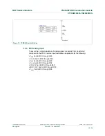
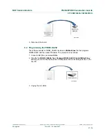
The V
AUX
regulator is always tied to the external PNP transistor
aaa-025589
Figure 10. V
AUX
regulator
5.2 V
CORE
settings and related configurations
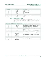
5.2.1 V
CORE
and F45xx versus FS65xx
The FS45xx family of devices only support V
CORE
LDO (low dropout) voltage regulators.
The FS65xx family only supports V
CORE
DC/DC voltage regulators. The evaluation
board circuitry accommodates this discrepancy by implementing a variation of the BOM
for each of the two device families. Populating or not populating resistors with some
components depends on which device family is in use and determines which network is
enabled.
For the FS45xx family, the following assembly options must be implemented:
•
R42: DNP
•
C8/C9/R4/D3/L2/C5/C7/R2/C11/R5/C17: populated
For the FS65xx family, it is the opposite: