


NXP Semiconductors
FS4500/FS6500 evaluation boards
KTFRDMFS4500-FS6500EVMUG
FS4500/FS6500 evaluation boards
All information provided in this document is subject to legal disclaimers.
© NXP B.V. 2017. All rights reserved.
User guide
Rev. 4.0 — 12 June 2017
11 / 34
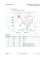
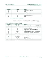
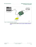
aaa-025546
.
Figure 6. Test points
Table 6. Test point definitions
Test point
name
Signal name
Description
TP1
GND
Ground
TP3
RXC
CAN receiver data. Logic level
TP4
INTB
INTB asserted (logic level = 0)
TP5
TXC
CAN transmit data. Logic Level
TP6
RXL
LIN receiver data. Logic level.
TP7
TXL
LIN transmit data. Logic Level
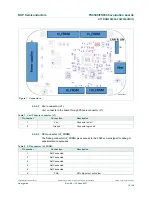
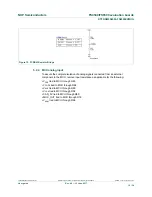
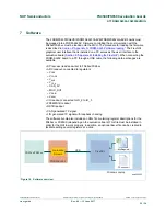
4.5.4 Connectors
Figure 7
shows the location of connectors on the board. The tables below list the pin-outs
for each connector.