


Programming Model
http://www.motorola.com/computer/literature
3-47
3
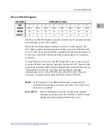
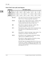
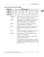
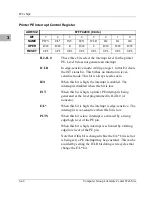
Printer Data Register
PD15-PD0
Writing to these bits causes the PCCchip2 to latch data
into the external printer data buffer. Generally the printer
data buffer only connects to PD7-PD0, because most
printer data paths are 8 bits wide.
PD7-PD0 can be accessed as an 8-bit register at location
$FFF4203B, or PD15-PD0 can be accessed as a 16-bit
register at location $FFF4203A.
In auto mode, writing these bits also generates the strobe
for the printer. Reading these bits causes the PCCchip2 to
read the data from the printer data signal lines (no strobe
is generated).
When the DOEN bit is set, the printer data signal lines are
driven by the external printer data buffer. When the
DOEN bit is cleared, they must be terminated to high or to
low and/or an external device must drive them.
ADR/SIZ
$FFF4203A (16-bits)
BIT
15-0
NAME
PD15 - PD0
OPER
R/W
RESET
X
Содержание MVME1X7P
Страница 1: ...MVME1X7P Single Board Computer Programmer s Reference Guide V1X7PA PG1 Edition of October 2000 ...
Страница 16: ...xvi ...
Страница 18: ...xviii ...
Страница 20: ...xx ...
Страница 26: ...xxvi ...
Страница 90: ...1 64 Computer Group Literature Center Web Site Programming Issues 1 ...
Страница 248: ...3 50 Computer Group Literature Center Web Site PCCchip2 3 ...
Страница 286: ...4 38 Computer Group Literature Center Web Site MCECC Functions 4 ...
Страница 288: ...A 2 Computer Group Literature Center Web Site Summary of Changes A ...
Страница 316: ...Index IN 14 Computer Group Literature Center Web Site I N D E X ...