HARDWARE DESCRIPTION
5-4
M68HC11EVB/D
5.2.3
Memory
The EVB memory map is a single map design. User RAM resides at different address locations to
that of the MCU ROM. Any code debugged in the RAM which is not re-locatable will require
modification before being transferred to EPROM and executed instead of the monitor (evaluation
mode).
To evaluate programs normally held in ROM, an 8k byte RAM is provided (socket U5). An
access time of 250 nanoseconds is necessary for a bus frequency of 2.1 MHz. Jumper headers J3
and J7 configure socket U4 for an additional 8k byte RAM supplied by the user if required. Refer
to paragraph 2.3.3 for additional memory select information.
5.2.4
Address Decoding/De-multiplexing
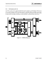
Address decoding is accomplished via a MC74HC138 device (U6) and is segmented into 8k byte
blocks. The low order address and data lines are de-multiplexed using a MC74HC373 device
(U2), to communicate with ROM, RAM, and the ACIA. The PRU uses a multiplexed input direct
from the MCU.
5.2.5
RS-232C I/O Port Interface Circuits
The EVB uses an MC68B50 ACIA device (U9) to communicate to a terminal via an RS-232C
driver/receiver interface (terminal I/O port). The terminal I/O port baud rate is hardware
selectable (300-9600 baud) via jumper header J5.
A second RS-232C driver/receiver interface (host I/O port) is fixed at 9600 baud via the MCU
SCI using a 2 MHz E clock external bus. This baud rate can be changed by software by
reprogramming the BAUD register in the ONSCI subroutine of the BUFFALO monitor program.
Refer to the buf25.asm file on the EVB diskette for additional information pertaining to the
ONSCI subroutine.
The host I/O port is provided for downloading Motorola S-records via the BUFFALO monitor
commands. When using the host I/O port, either by executing the HOST or LOAD commands,
The target system Serial Communications Interface (SCI) is switched to the host I/O port via the
MC74HC4066 digital switch device (U7) and MC74HC74 latch device (U11). The receiver
connection from the host I/O port is now connected to the RXD port of the MCU. The switching
of the receiver line from the target system to the host I/O port is accomplished by writing a logic
one in the bit 0 to any address in the range $4000-$5FFF. Likewise, writing a zero in bit 0 to any
address in the same range results in the target system being connected to the RXD pin of the
MCU.
As the RS-232C handshake lines are not used, a delay of approximately 300 milliseconds is
present between successive characters sent to the host computer during the execution of the
LOAD command in the monitor program.
Содержание M68HC11EVB
Страница 9: ...CONTENTS x M68HC11EVB D ...
Страница 35: ...MONITOR PROGRAM 3 8 M68HC11EVB D ...
Страница 81: ...OPERATING INSTRUCTIONS 4 46 M68HC11EVB D ...
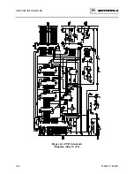
Страница 97: ...SUPPORT INFORMATION 6 12 M68HC11EVB D Figure 6 3 EVB Schematic Diagram Sheet 2 of 2 ...
Страница 103: ...APPLICATIONS B 2 M68HC11EVB D Figure B 1 Single Chip Mode Configuration ...

