background image

100

Mio336i PDA Maintenance

Mio336i PDA Maintenance

7.3 D.M. Test Introduction

7.3.1 Introduction of Diagnostic Manager

Diagnostic manager is used for verify hardware malfunction. It is an embedded system using Intel Cotulla and 
Microsoft Pocket PC 2002 operation system.

Diagnostic manager is based on Windows CE platform with multimedia capability. It equip with 64K color 
320*240 portrait reflective TFT LCD, touch screen input, one stereo audio out earphone Jack, one microphone and 
speaker for voice recording and playback, IrDA, RS232, USB, Jog wheel and some s/w application hot keys, 
proprietary extension sled port for versatile expansion capability, a Amber color battery charger LED and a Red 
color Notification LED. 

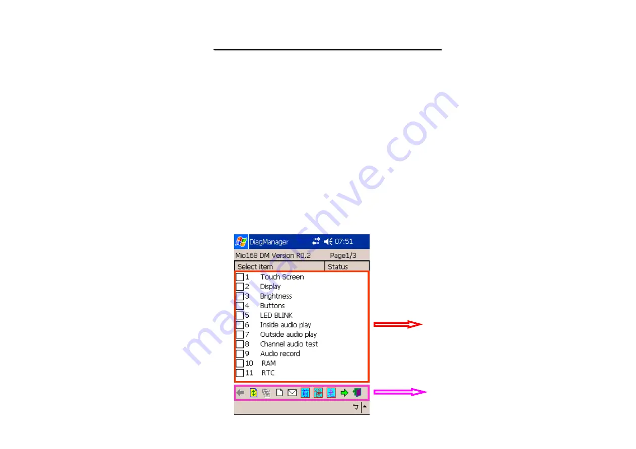
Fig. 1 : Snapshot of D.M.

Test menu

Tool bar

Содержание Mio336i

Страница 1: ...io336i Mio336i SERVICE MANUAL FOR SERVICE MANUAL FOR Mio336i Mio336i Mio336i Mio336i Mio336i Mio336i Mio336i Mio336i BY Sissel Diao Sissel Diao Repair Technology Research Department EDVD Repair Technology Research Department EDVD Nov 2003 ...

Страница 2: ...ration 1 3 Main System 1 4 Lithium Ion Rechargeable Battery CGA523450 Panasonic 1 5 GPIO Table 2 System View and Disassembly 2 1 Tools Introduction 2 2 System Views 2 3 System Disassembly 3 Definition Location of Connectors Major Components 3 1 Main Board 4 Pin Description of Major Components 4 1 Intel PXA255 Cotulla Application Processor 5 System Block Diagram 60 ...

Страница 3: ...ade 6 1 Burning IPL file Upgrade tool 6 2 Burning WinCE Image file 7 Mio336i Service TPI 7 1 Board Function Test 7 2 Run In Test 7 3 D M Test Introduction 8 Trouble Shooting 8 1 No Power 8 2 LCD No Display 8 3 LCD Display Abnormal 8 4 Memory Test Error 8 5 Audio Function Failure 8 6 Touch Screen Function Failure 9 Spare Parts List 100 ...

Страница 4: ...3 Mio336i PDA Maintenance Mio336i PDA Maintenance Contents 145 146 10 System Exploded Views 11 Circuit Diagram 12 Reference Material 164 ...

Страница 5: ... stereo audio out earphone Jack one microphone and speaker for voice recording and playback IrDA RS232 USB Joy stick and some s w application hot keys SD slot an Amber Green color battery charger LED and a Red color Notification LED 1 Hardware Engineering Specification 1 2 System Configuration CPU Intel PXA255 Cotulla 300MHz RAM 64MByte SDRAM K4S561633C RL 2 ROM 32Mbyte INTEL STRATA FLASH 28F256L3...

Страница 6: ...or LCD build in Touch Screen Transflective with LED backlight Charger controller TI BQ24010 Micro controller EM78P156ELAS USB Client for Window Active sync Serial Port IrDA Compatible with SIR 115 2Kbps SD MMC Microphone input Mono Earphone output Stereo Speaker output Mono IO Interface ...

Страница 7: ...wer amplifier TPA0253 Earphone Jack Stereo Audio codec WM9705 AC 97 interface 2 PWM BL_ON OFF 2 L R L R L R 24 576M XTAL When earphone inserted speaker output will be muted 5 Joystick Contact button Calendar button Record button Home button Task button Power button Micro Phone Input mono Host Address Bus SDRAM 103MHz 32Mbyte 2 Intel StrataFlash 28F256L30 K3 1 Host Data Bus SD Control data bus Gaug...

Страница 8: ...t can be shut down when it s not active TPS62000 ML4854 MP1521 Backlight Controller These part can be shut down when it s not active VCC_IN AAT3110 VCC_ 15 VCC_ 15 AIC1896 MOS Switch VCC_5V LCD Panel LCD Timing ASIC VCC3_LCD VCC3_LCD Can be turned OFF when display is OFF Flash 28F256L30 VCC1 8VSB MIC5207 Codec WM9705 Microphone MOS Switch MOS Switch VCC_AUD VCC_3VSB VCC_IN VCC_IN CPU I O PXA255 SD...

Страница 9: ...panion chips permit glueless connection to external devices An integrated LCD display controller provides support for displays and permits 1 2 and 4 bit grayscale and 8 or 16 bit color pixels A 256 byte palette RAM provides flexibility in color mapping A rich set of serial devices as well as general system resources provide enough compute and connectivity capability for many applications For detai...

Страница 10: ... Rich Serial Peripheral Set AC97 Audio port I2S Audio port USB client controller High speed UART Second UART with flow control FIR and SIR infrared comm ports Low Power Less than 500mW typical internal dissipation Supply voltage may be reduced to 0 85V Low power Sleep modes High Performance Memory Controller Four Banks of SDRAM up to 100MHz Five Static Chip Selects Support for PCMCIA or Compact Fl...

Страница 11: ...nance Additional Peripherals for System Connectivity Multimedia card controller MMC SSP controller I C controller Two Pulse Width Modulators PWMs All peripheral pins double as GPIOs Hardware Debug Features Hardware Performance Monitoring Features ...

Страница 12: ...H High Voltage Range PXA250 MHz 99 5 50 External Synchronous Memory Frequency Mid Range fSDRAM_M MHz 199 1 99 5 Turbo Mode Frequency Mid Range fTURBO_M V 1 10 1 00 0 90 VCC PLL_VCC Voltage Mid Range WCC_M Medium Voltage Range PXA250 and PXA210 MHz 99 5 50 External Synchronous Memory Frequency Low Range fSDRAM_L MHz 132 7 99 5 Turbo Mode Frequency Low Range fTURBO_L V 0 935 0 85 0 765 VCC PLL_VCC V...

Страница 13: ...stepping Core voltage frequency updated 1 65 1 43 1 32 1 155 Max 1 3 1 1 1 0 1 0 Typ 998 2 298 7 199 1 118 0 Max 1 235 99 5 1 045 99 5 0 95 99 5 0 95 99 5 Min Min VCC Volts Turbo Mode Frequency MHz Voltage and frequency Specifications Note 1 PXA255 PXA250 C stepping ID values updated 0x69264013 0x69052D06 A0 JTAG ID ARM ID Stepping PXA255 ID Values Package Introduction The applications processor i...

Страница 14: ... transactions are possible on every clock cycle Range of operating frequencies programmable burst length and programmable latencies allow the same device to be useful for a variety of high bandwidth high performance memory system applications Description 3 0V power supply LVTTL compatible with multiplexed address Four banks operation MRS cycle with address key programs CAS latency 1 2 3 Burst leng...

Страница 15: ... Extended Temperature Operation 25 C 85 C 54balls CSP Package Information VDD A2 A3 A4 A5 VSS J A10 A1 A0 A6 A7 A8 H CS BA1 BA0 A9 A11 A12 G WE RAS CAS CKE CLK UDQM F DQ7 LDQM VDD VSS NC DQ8 E DQ5 DQ6 VSSQ VDDQ DQ9 DQ10 D DQ3 DQ4 VDDQ VSSQ DQ11 DQ12 C DQ1 DQ2 VSSQ VDDQ DQ13 DQ14 B VDD DQ0 VDDQ VSSQ DQ15 VSS A 2 1 9 8 7 3 54Ball 6x9 CSP ...

Страница 16: ...VOL VOH VIL VIH VDD Output logic low voltage 2 4 Output logic high voltage 0 3 Input low voltage 2 2 Input logic high voltage 2 7 Supply voltage Min Parameter Recommended operation conditions Voltage reference to VSS 0V TA 25C 70C Commercial 25C 85C Extended Note 1 Pin to pin compatible SDRAM vender part number 1 SAMSUNG K4S561633C RL N 2 INFINEON HYB39L256160AC 3 MICRON MT48LC16M16LFFG ...

Страница 17: ... 13 ns Synchronous Burst Mode Reads 8 or 16 Words Wide 32 Word Write Buffer Buffered Enhanced Factory Programming K3 Architecture Multi Level Cell Technology High Density at Low Cost Symmetrical 64 K Word Blocks 256Mbit 256 Blocks 128Mbit 128 Blocks 64Mbit 64 Blocks Ideal for CODE DATA applications K3 Packaging and Voltage 64 Ball Intel Easy BGA Package 56 and 79 Ball Intel VF BGA Package VCC 2 70...

Страница 18: ...o allows two processors to interleave code operations while program and erase operations take place in the background The 1 8 Volt Intel StrataFlash wireless memory with 3 Volt I O device is manufactured using Intel 0 13 Ìm ETOX VIII process technology It is available in industry standard chip scale packaging L30 High performance Read While Write Erase 85 ns initial access 52MHz with zero wait sta...

Страница 19: ...eration I O voltage 2 2 V 3 3 V Standby current 30 µA Typ 4 Word synchronous read current 17 mA Typ 54 MHz L30 Software 20 µs Typ program suspend 20 µs Typ erase suspend Intel Flash Data Integrator FDI optimized Basic Command Set BCS and Extended Command Set ECS compatible Common Flash Interface CFI capable L30 Security OTP space 64 unique device identifier bits 64 user programmable OTP bits Addit...

Страница 20: ...ividual block lock down L30 Quality and Reliability Expanded temperature 25 C to 85 C Minimum 100 000 erase cycles per block ETOX VIII process technology 0 13 µm L30 Density and Packaging 64 128 and 256Mbit density in VF BGA packages 128 0 and 256 0 Density in Stacked CSP 16 bit wide data bus ...

Страница 21: ...on and S PDIF output Headphone auto detect I S output and headphone buffer on the mono output are included Additionally the WM9705 integrates a complete 4 wire touch screen controller including on chip screen drivers pen down detection feature and pressure measurement capability A 5 pin digital bi directional AC Link serial interface allows transfer of control data and DAC and ADC words to and fro...

Страница 22: ...interface with co ordinate and pressure measurement and pen down detection Wake up from sleep mode on pen down 3V to 5V operation Extensive power management features including hardware power down option Standard AC 97 pinout in 48 pin TQFP package or 48 pin QFN package Recommended operating temperature 25 85 ºC Ta ...

Страница 23: ...to a 8Ω speaker The gain of the input stage is set by the user selected input resistor and a 50kΩ internal feedback resistor AC RF RI The power stage is internally configured with a gain of 1 25V V in SE mode and 2 5V V in BTL mode Thus the overall gain of the amplifier is 62 5kΩ RI in SE mode and 125kΩ RI in BTL mode The input terminals are high impedance CMOS inputs and can be used as summing no...

Страница 24: ...e Power Supply Compatibility 2 5 V to 5 5 V Low Supply Current 3 2 mA Typical at 5 V 2 7 mA Typical at 3 V Shutdown Control 1 uA Typical Shutdown Pin is TTL Compatible 40 C to 85 C Operating Temperature Range Space Saving Thermally Enhanced MSOP Packaging ...

Страница 25: ... 2 8 mm wide x 1 9 mm high Extended operating temperature range 30 ºC to 85 ºC Internal current source eliminates need for a current limiting resistor for IR LED Meets IEC 825 1 Class 1 eye safety specifications Features Block Diagram Transmission distance 1 m Transmission angle 15 Test criteria I O I O Shield connection IRED anode Transmitter input Receiver output Function 7 6 5 Pin TAB LEDA TXD ...

Страница 26: ...receiver device ideal for laptop notebook computer and PDA applications The SP3243E includes one complementary receiver that remains alert to monitor an external device s Ring Indicate signal while the device is shutdown The Auto Online feature allows the device to automatically wake up during a shutdown state when an RS 232 cable is connected and a connected peripheral is turned on Otherwise the ...

Страница 27: ...o336i PDA Maintenance Enhanced ESD specifications 15KV human body model 15KV IEC1000 4 2 air discharge 8KV IEC1000 4 2 contact discharge 28 pin SSOP derate 11 2mW ºC above 70 ºC 900mW Operation temp 0 ºC to 70 ºC Power Dissipation ...

Страница 28: ...2 8 LCD Timing Controller NL2432DR22 For NEC Panel Features Operating Temperature Range 25 75 C Supply Voltage Range 2 5 3 6V Power Consumption 10mW DCK 6 36MHz VDD 3 3V Package Package Type TQFP Number of Pin 80 pins Size L x W x T 12 1mm x 12 1mm x 1 1mm ...

Страница 29: ...ata Green Bit2 7 5MHz IBC I GI2 13 Input Data Green Bit3 7 5MHz IBC I GI3 12 Input Data Green Bit3 7 5MHz IBC I GI3 11 Input Data Green Bit4 7 5MHz IBC I GI4 10 Input Data Green Bit5 7 5MHz IBC I GI5 9 Input Data Blue Bit0 7 5MHz IBC I BI0 8 GND Terminal P GND 7 IBC Input Data Blue Bit1 Input Data Blue Bit2 Input Data Blue Bit3 Input Data Blue Bit4 Input Data Blue Bit5 Supply Voltage 2 3V to 3 6V ...

Страница 30: ...a Inversion Signal 7 5MHz 40pF 2mA OB1T O INV 34 Source Driver Output Enable Signal 18 75MHz 40pF 2mA OB1T O HOE 33 Polarity Change 18 75KHz 40pF 2mA OB1T O PC 32 Supply Voltage 2 3V to 3 6V P VDD 31 Power On Clear 0 reset 1 reset off IBH I POC 30 Gate Driver Output Enable Terminal DC IBCD1 I OEN 29 TEST Terminal 0 Normal 1 Test Mode DC P TSTEN2 28 Data Enable Signal 18 75MHz IBC I DE 27 GND Termi...

Страница 31: ... Red0 7 5MHz 40pF 2mA OB1T O RO0 56 Output Data Green Bit5 7 5MHz 40pF 2mA OB1T O GO5 55 Supply Voltage 2 3V to 3 6V P VDD 54 Output Data Green Bit4 7 5KHz 40pF 2mA OB1T O GO4 53 Output Data Green Bit3 7 5MHz 40pF 2mA OB1T O GO3 52 Output Data Green Bit2 7 5MHz 40pF 2mA OB1T O GO2 51 Output Data Green Bit1 40pF 2mA OB1T O GO1 50 Output Data Green Bit0 7 5MHz 40pF 2mA OB1T O GO0 49 Output Data Blue...

Страница 32: ...4 Switching Resolution Set up Terminal 0 DC IBCD1 I PANS0 73 Switching Resolution Set up Terminal 1 DC IBCD1 I PANS1 72 Polarity Inversion 0 Line Reverse 1 Frame Reverse DC IBCD1 I PC1 71 Source Driver Switching Set up Terminal DC IBCD1 I DSE 70 HOE Pulse Width Selecting Function DC IBCD1 I HOEPW 69 GND Terminal V Driver Start Pulse Mark 71Hz Frequency 40pF Capacity 2mA Output Current OB1T I O Buf...

Страница 33: ...signal electrode a driving circuit This module s consist of LCD panel Driver Back light and Touch panel The 8 9cm 3 5Type diagonal display area contains 240 320 pixels and can display 262 144 colors simultaneously Description Transflective type Back light and touch panel attached Recommended LCD controller part No SIL50282F23k100 NEC corp High Brightness High contrast ratio Small footprint and lig...

Страница 34: ...lue vertical stripe Pixel arrangement mm 0 2235 H x 0 2235 V Pixel pitch mm 0 0745 H x 0 2235 V Dot pitch Pixel 240 H x 320 V Number of pixels Mm 53 64 H x 71 52 V Diagonal display area 8 9cm Type 3 5 Display area Mm 64 0 0 3 H x 85 0 0 3 V x 3 96 TBD D Module size Units Specification Item General Specification ...

Страница 35: ... 0 3xVCC 0 VIL Logic input low voltage Logic signal V VCC 0 7xVCC VIH Logic input high voltage V 14 0 15 0 16 0 VGOFF V driver supply voltage V 16 0 15 0 14 0 VGON V driver supply voltage V TBD 4 5 TBD VDD H driver supply voltage V 3 6 3 0 2 6 VCC Logic supply voltage Remarks Units Max Typ Min Symbols Parameters Electrical Characteristics Note 1 An optional value for COM C is in the range of 1 5 t...

Страница 36: ...1 5 Ylin Line linearity Y direction 1 5 Xlin Line linearity X direction Ohm 950 350 Ry Resistor between terminals YU YD Ohm 900 300 Rx Resistor between terminals XL XR V 5 5 Vtp Touch panel input voltage Remarks Units Max Typ Min Symbols Parameters 3 Touch panel Ta 25 C Supply Voltage Sequence V 90 0V 0 0 90 0 0 0 90 I VGON VDD and V0 to V4 VCC OEN Logic signals VGOFF ...

Страница 37: ...ed on minimum current An internal charge timer provides a backup safety feature for charge termination The bqTINY_ automatically re starts the charge if the battery voltage falls below an internal threshold The bqTINY_ automatically enters sleep mode when VCC supply is removed In addition to the standard features different versions of the bqTINY_ offer a multitude of additional features These incl...

Страница 38: ... Reverse Leakage Protection Prevents Battery Drainage Integrated Current and Voltage Regulation 0 5 Voltage Regulation Accuracy Charge Termination by Minimum Current and Time Precharge Conditioning With Safety Timer Status Outputs for LED or System Interface Indicates Charge and Fault Conditions Battery Insertion and Removal Detection Works With Regulated and Unregulated Supplies Short Circuit Pro...

Страница 39: ...veloping and verifying user s programs Moreover user can take advantage of EMC writer to easily program his development code In Mio336i PDA EM78P156 is used to sense main battery capacity and inform CPU If main battery capacity is under which we set micro controller will take related action to force system into sleep mode And if main battery is still under the protection level micro controller wil...

Страница 40: ...8 8 bits on chip registers SRAM general purpose register 2 bi directional I O ports 5 level stacks for subroutine nesting 8 bit real time clock counter TCC with selective signal sources trigger edges and overflow interrupt Two clocks per instruction cycle Power down SLEEP mode Three available interruptions TCC overflow interrupt Input port status changed interrupt wake up from sleep mode External ...

Страница 41: ...en drain pins 2 programmable R option pins Package types 18 pin DIP 300mil EM78P156ELP 18 pin SOP SOIC 300mil EM78P156ELM 20 pin SSOP 209mil EM78P156ELAS 99 9 single instruction cycle commands The transient point of system frequency between HXT and LXT is around 400KHz ...

Страница 42: ...ge use P52 CHARGE_DET1 detect main is charging or not P53 AC_IN Detect AC adapter is inserted or not P60 MP_WAKE To force Micro P to be wake up from sleep mode when hot key is pressed P61 GAUGE0 Indicate battery capacity to CPU P62 GAUGE1 Indicate battery capacity to CPU P63 GAUGE2 Indicate battery capacity to CPU P64 RST_MCU Reserve P65 PWRCORE_EN Indicate system is in RUN mode or not P66 BAT_FAU...

Страница 43: ... memory organized as 16 x 8 with a 2 wire serial inter face Low voltage design permits operation down to 1 8 volts for the 24xx00 version and every version maintains a maximum standby current of only 1mA and typical active current of only 500mA This device was designed where a small amount of EEPROM is needed for the storage of calibration values ID numbers or manufacturing information etc The 24x...

Страница 44: ...and 400kHz 5V compatibility Self timed write cycle including auto erase 4 ms maximum byte write cycle time 1 000 000 erase write cycles guaranteed ESD protection 4kV Data retention 200 years 8L DIP SOIC TSSOP and 5L SOT 23 packages Temperature ranges available Commercial C 0 to 70 Industrial I 40 to 85 Automotive E 40 to 125 Block Diagram ...

Страница 45: ...in HP insert detect NA Pin 6 Earphone L channel Input Pin 3 Pin 5 Earphone R channel Input Pin 2 Pin 4 Earphone Jack GND Pin 1 Earphone Jack KM03011ABG Pin Assignment SDCLK Pin 5 SDDATA2 Pin 9 VDD Pin 4 SDDATA1 SDDATA0 GND Pin 8 GND Pin 3 Pin 7 SDCMD Pin 2 Pin 6 SDDATA3 Pin 1 SD Connector Honda SD DR9LFYGD Pin Assignment ...

Страница 46: ...ty Reduction Max 0 500mA Current Consumption V 10V Maximum operating Voltage V 3 0V Standard Operating Voltage S P L 120dB Max Input Sound Level Hz 100 10 00Hz Frequency Range Less than 2 200kΩ Impedance 0dB 1 V Pa 1kHz 38 4 0 dB Sensitivity CHRG DIA FOIL Electret Type Notes Specification Values Characteristic OMNI Directional Directional Characteristic Electrical Specifications Operating temperat...

Страница 47: ...l clock only The power consumption due to PLL is excluded IDLE mode the block disconnects clocks FCLK only to the CPU core while it supplies clocks to all other peripherals The IDLE mode results in reduced power consumption due to CPU core Any interrupt request to CPU can be woken up from the Idle mode Power OFF mode the block disconnects the internal power So there occurs no power consumption due...

Страница 48: ...on 1 3 5 2 POWER_OFF Mode The block disconnects the internal power So there occurs no power consumption due to CPU and the internal logic except the wake up logic in this mode Activating the Power OFF mode requires two independent power sources One of the two power sources supplies the power for the wake up logic The other one supplies other internal logics including CPU and should be controlled f...

Страница 49: ...mal mode and Power off mode And when you press this button more than 1 sec while system is operating panel front light will be Turn ON OFF 1 3 6 2 Record Button This button is used to record voice when user is pressing it When user pressed AP will be launched 1 3 6 3 Reset Button This button is used to reset PDA This reset function will not erase user data information after this button is pressed ...

Страница 50: ... PDA Maintenance Mio336i PDA Maintenance 1 3 6 4 AP function Buttons Task My menu Calendar Contact 1 3 6 5 Buttons for 4 way key and Enter use Joystick Up Joystick Down Joystick Left Joystick Right Joystick Enter ...

Страница 51: ...in 17 Pin 16 Pin 15 Pin 14 Pin 13 Pin 12 RTS Pin 11 TXD Pin 10 DCD Pin 9 DSR Pin 8 CTS Pin 7 RXD Pin 6 USB_CRADLE_DET Pin 5 GND Pin 4 USB0_P Pin 3 USB0_N Pin 2 GND Pin 1 Note 1 Pin 18 is used for cradle LED When PDA is plugged into cradle the LED will be lighted Note 2 Pin 16 17 are used for cradle charge current detect The cradle micro P can detect these 2 pins to control the charge current in cr...

Страница 52: ...r CGA523450 Battery Pack Characteristics and performance 0 2C discharge Remark Approx 20g Weight 1700mA Discharging Current Max 2hours Charging Time Std 4 2V Charging Voltage 850mA Charging Current Std 2 75V End Voltage 3 6V Nominal Voltage 900mAh 850mAh Min Capacity Specification Item Temperature 20 5 degree C Dimensions w Tube 50mm T x 34mm W x 5 25mm H ...

Страница 53: ...52 Mio336i PDA Maintenance Mio336i PDA Maintenance ...

Страница 54: ...AY_ UP BT_FOURWAY_ UP GPIO_13 CONTACT BUTTON YES H L I CONTACT CONTACT GPIO_12 SD interface H L I O SDDATA3 SDDATA3 GPIO_8 TASK BUTTON YES H L I TASK TASK GPIO_7 L SD clock output Record Button MEMEO BUTTON SD card insertion detect pin USB cable detect pin when it s inserted Record button detect Power button to control system ren sleep and black light ON OFF Description YES YES YES YES YES YES Int...

Страница 55: ...creen interrupt H H I IRQ_PEN IRQ_ PEN GPIO_32 AC97 INTERFACE H L O AC97_SYNC AC97_SYNC GPIO_31 During boot up this pin is output After boot up this pin is input for Main Second battery gauge select H I O BAT M S BAT_M S GPIO_27 M B battery Gas Gauge pin H I GAUGE2 GAUGE2 GPIO_26 M B battery Gas Gauge pin M B battery Gas Gauge pin Adapter detect pin when it s inserted Cold boot detect pin when sys...

Страница 56: ...IO_55 Card control H SA_PSKTSE GPIO_54 Card control H SA_PCE2 GPIO_53 Card control H SA_PCE1 GPIO_52 Card control H SA_PIOW GPIO_51 Card control H SA_POR GPIO_50 IrDA RX pin H I IR_RXD IR_RXD GPIO_46 SD card write protect pin L H I SD_WP BT_RTS GPIO_45 CPU battery fault Main battery charge detect pin Switch board Blue LED control pin COM port signal COM port signal Description Interrupt wake up H ...

Страница 57: ..._70 For LCD control signal H L O LCD_MCK LCD_MCK GPIO_76 LCD HSYNC signal O GPIO_75 LCD VSYNC signal H O VSYNC DCD WAKE GPIO_74 LCD data signal H L O LCD_R1 LCD R1 GPIO_73 LCD data signal H L O LCD_R5 LCD R5 GPIO_72 LCD data signal H L O LCD_R4 LCD R4 GPIO_71 LCD data signal H L O LCD_G5 LCD G5 GPIO_67 LCD data signal L L O LCD_G4 LCD G4 GPIO_66 L LCD data signal LCD data signal LCD data signal LC...

Страница 58: ...lt Open Drain pin X H L O BAT_FAULT_IR Q BAT_FAULT_IR Q P67 Micro P Battery fault Open Drain pin X H L O BAT_FAULT_MC U SA_BATT_FAUL T P66 M B battery Gas Gauge pin X I O GAUGE1 GAUGE1 P62 M B battery Gas Gauge pin X I O GAUGE0 GAUGE0 P61 Key press interrupt AC detect Main battery charge detect pin Reserve for detect second battery Detect Main battery Description Interrupt wake up X X X X X I O St...

Страница 59: ...c power enable pin X H L O AUD_PWR_ON AUD_PWR_ON 2Q6 SA_D13 Amplifier power enable pin X H H O AMP_PWR_ON AMP_PWR_ON 2Q8 SA_D15 VCORE2 2Q5 SA_D12 VCORE1 2Q4 SA_D11 USB power enable pin when USB cable is inserted LCD data output enable control pin Description Interrupt wake up X L X L I O State Reset Sleep Mode Status O O I O pin USB_EN LCD_ON Signal name Mio338 H H H L activity SW_RED 2Q3 SA_D10 U...

Страница 60: ... Tools Introduction 2 System View Disassembly 2mm 2mm Bit Size 0 Screw Size Tooling Tor Bit Size 1 M2 0 Auto Screw driver 2 0 2 5 kg cm2 0 2 Auto screw driver for PDA assembly disassembly 1 Minus screw driver with bit size 2mm for PDA assembly disassembly ...

Страница 61: ...nce Mio336i PDA Maintenance 2 2 System View 2 2 1 Top View Note Button Internal MIC Contacts Button Left Right Up Down Button Calendar Button Internal Speaker Task Button 2 2 2 Front View Cradle Connector Power LED Indicator ...

Страница 62: ...61 Mio336i PDA Maintenance Mio336i PDA Maintenance 2 2 3 Left Side View Power Button Record Switch External Ear Phone Jack 2 2 4 Right Side View Reset Switch ...

Страница 63: ...62 Mio336i PDA Maintenance Mio336i PDA Maintenance 2 2 5 Rear View STYLUS Pen 2 2 6 Bottom View SD MMC Memory Connector IrDA COLD BOOT Switch ...

Страница 64: ...esponding illustrations Use the chart below to determine the disassembly sequence for removing components from the PDA NOTE Before you start to install replace these modules disconnect all peripheral devices and make sure the PDA is turned off and disconnected to AC Adaptor 2 3 1 Rear Cover 2 3 2 Battery Pack 2 2 3 Main Board 2 3 4 LCM Module Main Modular Components ...

Страница 65: ... if connected on the PDA Then remove the STYLUS Pen Figure 2 1 4 Remove four screws that secure the rear cover ASSY Figure 2 2 5 Lift up the rear cover ASSY Figure 2 3 Figure 2 1 Remove the STYLUS Pen Figure 2 2 Remove four screws Figure 2 3 Remove rear cover Reassembly 1 Make sure the rear cover ASSY is assembly correctly to the MID Frame and secured four screws 2 Insert the STYLUS Pen and SD MMC...

Страница 66: ... rear cover Refer to section 2 3 1 Disassembly 2 Disconnect the battery pack cable Figure 2 4 3 Lift up the battery pack Reassembly 1 Place the Battery Pack into the compartment and reconnect the cable 2 Replace the rear cover Refer to section 2 3 1 Reassembly Figure 2 4 Remove the battery pack ...

Страница 67: ... Figure 2 5 3 Remove one screw that secure the board Figure 2 6 4 Carefully remove the main board Figure 2 7 Disassembly Reassembly 1 Fit the main board and secure with one screw 2 Reconnect the LCM s cable to main board 3 Remove the battery pack and rear cover Refer to sections 2 3 1 and 2 3 2 Disassembly Figure 2 6 Remove one screw Figure 2 5 Disconnect the LCM s cable Figure 2 7 Separate the MB...

Страница 68: ...2 3 1and 2 3 2 Disassembly 2 Remove the main board Refer to section 2 3 4 Disassembly 3 Carefully separated the two lock on the MID Frame that fasten the LCM Module and slightly lift up the LCM Module Figure 2 8 4 Now you can remove the LCM module Figure 2 9 Figure 2 8 Separate the LCD module from the MID frame Figure 2 9 lift up the LCM module ...

Страница 69: ... Module to the MID Frame and secured the two lock well 2 Place the MB to the MID Frame Secured one screws to fasten MB on MID Frame well Refer to 2 3 3 Reassembly 3 Reassembly the battery pack Refer to section 2 3 2 Reassembly 4 Reassembly the rear cover Refer to section 2 3 1 Reassembly ...

Страница 70: ...a Microprocessor U3 U5 K4S561633C RL 32MB SDRAM U4 NOR Flash ROM U11 WM9705 Audio Codec U16 RS232 U18 IrDA Module U19 SIL50282F23K100 NEC LCD Controller U23 EM78P156ELAS Micro Controller SW1 Reset Switch SW3 JOYSTICK Switch SW4 TASK Switch SW5 MEMO Switch SW6 CALENDAR Switch SW7 CONTACT Switch U5 U3 U1 U4 U11 SW3 U16 U19 U23 U18 SW1 SW5 SW7 SW4 SW6 ...

Страница 71: ...n of Connectors Major Components U36 Extend GPIO Controller J2 External Ear phone Connector J4 LCM Panel Connector J5 SD Slot Compatible with MMC memory card Connector J6 Battery Connector J8 Cradle Connector SW2 Power Switch SW8 Power Button SW9 Recording Button J5 SW2 J4 J2 SW8 SW9 U36 J6 J8 ...

Страница 72: ...e for static interface output Signals that the current transaction is a read or write Signal Name Type Description SDCLK 1 OCZ SDCLK 2 OC SDRAM Clocks output Connect SDCLK 1 and SDCLK 2 to the clock pins of SDRAM in bank pairs 0 1 and 2 3 respectively They are driven by either the internal memory controller clock or the internal memory controller clock divided by 2 At reset all clock pins are free...

Страница 73: ...ata output Transfers pixel information from the LCD controller to the external LCD panel RTC clock output Real time clock 1Hz tick L_DD 13 14 GPI O 71 72 ICOCZ LCD display data output Transfers pixel information from the LCD controller to the external LCD panel 3 6864 MHz 32 KHz clock output Output form 3 6864 MHz 32 KHz oscillator L_DD 15 GPIO 7 3 ICOCZ LCD display data output Transfers pixel inf...

Страница 74: ...RAM GPI O 82 ICOCZ Network synchronous serial port frame output input NSSPTXD GPIO 8 3 ICOCZ Network synchronous serial port transmit receive output input Signal Name Type Description NSSPRXD GPIO 8 4 ICOCZ Network synchronous serial port transmit receive output input USB Client Pins USB_P IAOAZ USB client positive bi directional USB_N IAOAZ USB client negative pin bi directional AC97 Controller a...

Страница 75: ...sertion terminates the current instruction abnormally and causes a reset When nRESET is driven high the processor starts execution from address 0 nRESET must remain low until the power supply is stable and the internal 3 6864 MHz oscillator has stabilized Signal Name Type Description PWR_EN OC Power enable for the power supply output When negated it signals the power supply to remove power to the ...

Страница 76: ...A255 Cotulla Processor U3 U5 64MByte SDRAM U4 32MByte NOR Flash U11 Audio Codec U15 Audio Amplifier J5 SD Card Socket Speaker U18 IrDA P3 P4 P7 P7 P6 P6 P11 P8 J7 LCM Connector P9 U19 LCD Timing Controller U16 RS232 Controller J8 Cradle Connector P9 P8 P15 5 System Block Diagram ...

Страница 77: ...hould burn IPL Upgrade tool to your device first use the Parallel port to PDA JTAG cable Then the WinCE image can be flashed by Upgrade tool The system requirement shows as below table Parallel port to PDA JTAG cable Parallel port to PDA JTAG cable Parallel port to PDA JTAG cable Mio336i PDA Hardware Windows 2000 Jflash_new exe 336UTR11 bin Giveio Driver for Windows 2000 Software PIN 2 TDI PIN 18 ...

Страница 78: ... step by step to do the burning IPL process 1 Copy all related files of Giveio driver to C WINNT System32 Drivers folder and then use the hardware wizard to install the giveio port Figure 6 1 2 Setup the Giveio driver to system A Initial Parallel port to JTAG Tool Figure 6 1 Copy Giveio driver to system ...

Страница 79: ...ur desktop PC and the other JTAG side of the cable please connect to the Mio336i PDA correctly and keep Cold Boot Button ON 2 Key in C jflash_new I 336UTR11 bin in Start Run CMD mode Figure 6 2 B Burning IPL Initial Programmable Logic file Factory used Figure 6 2 Key in C jflash_new I 336UTR11 bin in Start Run CMD mode ...

Страница 80: ...Figure 6 4 4 After Upgrade Tool Menu show ROM Upgrade OK Restart your device Figure 6 4 C Upgrade it by SD MMC Memory Third parity used Figure 6 4 Select 1 Image Upgrade SD MMC 1 WinCE Image SD MMC Upgrade Tool V1 1 0 WinCE Image USB 2 UBoot Image USB 3 UBoot Image SD MMC 4 BIN Image USB 5 Flash Type 6 Reboot Choice 1 Figure 6 3 Format SD MMC Memory Card to FAT16 format Figure 6 5 Cold Boot the PD...

Страница 81: ...when Abnormal or upgrading WinCE system There are two ways for WinCE image Upgrade process A By Cradle to USB Cable or B By SD MMC Memory 1 Connect the USB to Cradle cable Install the USB Cradle cable driver to PC Figure 6 6 A Upgrade it by Cradle to USB Cable Figure 6 6 Install USB to Cradle cable driver to PC ...

Страница 82: ...SB 1 WinCE Image SD MMC 2 UBoot Image USB 3 UBoot Image SD MMC 4 BIN Image USB 5 Flash Type 6 Reboot Choice 0 2 Install the ActiveSync 3 7 and disable the ActiveSync setting of USB connection Figure 6 7 3 Hold the Jog Wheel Down Cold Boot to Cold Boot the PDA system and enter the Upgrade Tool Menu Figure 6 8 4 Execute the file named RomUpdate_RD_R01 exe at the PC side Figure 6 9 Figure 6 9 Execute...

Страница 83: ...ct USB item in Upgrade tool Menu by Jog Wheel Action and Click the next Figure 6 11 7 Select WinCE image file for update image And wait for few minutes Figure 6 12 Figure 6 10 Click the next and follow the instruction Figure 6 11 Select USB item in Upgrade tool Menu by Jog Wheel Action and Click the next Figure 6 12 Select WinCE image file ...

Страница 84: ...start your device Select Finish on your PC side Figure 6 14 Upgrade Tool V1 1 0 WinCE Image USB 1 WinCE Image SD MMC 2 UBoot Image USB 3 UBoot Image SD MMC 4 BIN Image USB 5 Flash Type 6 Reboot Choice 0 WinCE USB Upgrade Flashing finished ROM Upgrade OK Restart your device Figure 6 13 Please don t interact with your PDA unless instructed to do so Figure 6 14 Cold Boot the PDA ...

Страница 85: ...e SD MMC Figure 6 16 4 After Upgrade Tool Menu show ROM Upgrade OK Restart your device Figure 6 17 B Upgrade it by SD MMC Memory Figure 6 16 Select 1 Image Upgrade SD MMC 1 WinCE Image SD MMC Upgrade Tool V1 1 0 WinCE Image USB 2 UBoot Image USB 3 UBoot Image SD MMC 4 BIN Image USB 5 Flash Type 6 Reboot Choice 1 Figure 6 15 Format SD MMC Memory Card to FAT16 format Figure 6 17 Cold Boot the PDA Up...

Страница 86: ...rvice TPI 7 1 Board Function Test 7 1 1 Test Items 1 Touch Screen 2 Display 3 Brightness 4 Buttons 5 LED 6 Audio play 7 Channel Audio play 8 Audio recorder 9 RAM 10 RTC 11 CPU 12 SIO 13 USB 14 Slave IrDA 15 SD MMC 16 GPS 17 Flash ROM 18 Idle Off 19 Suspend 20 Reset ...

Страница 87: ...ntenance 7 1 2 Test Equipments Name 1 Headphone 2 SD MMC Card 3 PDA 4 PC 5 Serial Sync cable 6 Touch Pen 7 NEC Touch Panel 8 USB Cable AC Adapter 7 1 3 Test Programs 1 PDA D M Mio168DM exe 2 PC Windows 2000 ActiveSync Quantities 1 1 1 1 1 1 1 1 ...

Страница 88: ... Mio336i PDA Maintenance 7 1 4 Test Flow Chart Record Error Status Repair R Start Power on Backlight Serial Enter WinCE Button Y Y Y Y Y R N R N R N R N USB Y R N Audio DM 8 words SD MMC Y Y Y Y R N R N R N R N IR Y R N End R N ...

Страница 89: ... Cold Boot to boot strap flip the screen to enter WinCE Check the picture is normal or not if it is abnormal test is fail otherwise test is pass 2 Button function test Record Reset JOYSTICK up down enter left right Contact Task Calendar Note Press the each Button in turn and check the picture is accord to the button see the figure figure is only the below five items Contact Calendar Note Task JOYS...

Страница 90: ...er key function is normal or not Flip Start Setup System Backlight turn the backlight from dark to bright then turn to the middle to check the bright of screen is change or not if it is then test pass See the follow figure 4 Serial port function test suspend the PDA before test connect the serial cable to PDA If the ActiveSync3 7 connect success then test is pass ...

Страница 91: ...90 Mio336i PDA Maintenance Mio336i PDA Maintenance 5 USB function test connect the USB cable to PDA If the ActiveSync3 7 connect success then test is pass See the follow figure ...

Страница 92: ...91 Mio336i PDA Maintenance Mio336i PDA Maintenance 6 IR function test distance 50cm flip Increase Create Note file send and receive See the follow figure ...

Страница 93: ...92 Mio336i PDA Maintenance Mio336i PDA Maintenance 7 Flip Increase write one 田 word in Note to test cardiogram phenomena then write four 8 words ...

Страница 94: ...m the File Explorer Repeat this action two times and enter SD card copy the MP3 music to My documents to check the PDA is die or not If it can copy and file size is not change test is pass otherwise test is fail 9 Record test press record button distance 20 30 centimeter say one two three play this recording sound Inside speaker and earphone each time If plug in earphone the outside speaker is not...

Страница 95: ...94 Mio336i PDA Maintenance Mio336i PDA Maintenance 10 Play test play Windows Media notice the sound is normal or not ...

Страница 96: ...ogram test Touch Screen Display Brightness Buttons LED BLINK Inside audio play Outside audio play Channel audio test Audio record RAM RTC VR H Pattern CPU SD MMC GrayScale Panel each item need test pass Note When test Channel audio the inside speaker and outside earphone need test pass ...

Страница 97: ...t 7 2 1 Test Items Battery Calibration 7 2 2 Test Equipments Name 1 Touch Pen 2 SD MMC Card 3 USB Cable AC Adapter Quantities 1 1 1 7 2 3 Test Programs Need the follow program in SD MMC Card 1 RUN folder there has movie file in the folder 2 autorun exe 3 SQDMT6d exe ...

Страница 98: ...97 Mio336i PDA Maintenance Mio336i PDA Maintenance 7 2 4 Test Flow Chart Start Enter WinCE Auto Test Power on Cycle 4 hours End Note Charge 3 hours Discharge 1 hours ...

Страница 99: ...98 Mio336i PDA Maintenance Mio336i PDA Maintenance 7 2 5 Test Process 1 Enactment The main battery capacity should not full in power picture ...

Страница 100: ...y Calibration item to enter figure 2 b Plug in USB cable with power cable the charge LED indicate Red When charge three hours charge full the LED indicate Green discharge one hours then Battery Life Percent is not 100 If the main battery capacity is not full test is pass If it is full discharge at this station and put the backlight to the brightest replay movie 15 minutes If it has change then tes...

Страница 101: ...tic manager is based on Windows CE platform with multimedia capability It equip with 64K color 320 240 portrait reflective TFT LCD touch screen input one stereo audio out earphone Jack one microphone and speaker for voice recording and playback IrDA RS232 USB Jog wheel and some s w application hot keys proprietary extension sled port for versatile expansion capability a Amber color battery charger...

Страница 102: ...ntroduce each item The result of test menu will show in the status display and log file if the result is correct it will show PASS otherwise show FAIL Some of items will create a new window or dialog box if user doesn t operate in specific time at left upper corner show counter it will show NOP To test the item check the checkbox to un select the test item remove the check of the checkbox ...

Страница 103: ...en function Test method Press the center of the cross tag and follow the instruction There are four cross tag on the each corner After that the panel will show the X Y coordinate on bottom while you press any place of the touch screen Criteria If any tap over 10 offset with default value the test fails ...

Страница 104: ...Test method When select the item system creates a new window the windows display 4 colors red green blue yellow and display sequence by random Then DM creates a dialog box ask user to select touch screen which it assigns color Criteria If user selected an area which color was assigned by dialog It will show PASS otherwise show FAIL ...

Страница 105: ...ion Test method When select the item system creates a new window in the center of windows show the brightness degree When system starts brightness degree will from dark to light of light to dark by random Then system creates a dialog box ask user answer Criteria If answer is correct show PASS otherwise show FAIL ...

Страница 106: ... function Test method When select the item system creates a new window and user should tap button follow step If it matches system will show OK in status area if it s not then show Fail Button test sequence is fixed as picture as below Criteria If all items are OK show PASS otherwise show FAIL ...

Страница 107: ...7 3 2 5 LED Purpose Verify the LED function Test method When select the item notification LED glitter several times then system create a dialog box and ask user that Did notification LED glitter Criteria If answer is correct show PASS otherwise show FAIL ...

Страница 108: ...hone When select items you can hear one of 3 different types of sounds decided by random from earphone there are 3 different type of animal sound dog cat and chicken Then system creates a dialog box and asks user which sound user heard Criteria In the Inside audio out and Outside audio out test item If answer is correct show PASS otherwise show FAIL ...

Страница 109: ...ect items you can hear one of 3 different type of sounds decided by random from speaker there are 3 different type of animal sound dog cat and chicken Then system creates a dialog box and asks user which sound user heard Criteria In the Inside audio out and Outside audio out test item If answer is correct show PASS otherwise show FAIL ...

Страница 110: ... random from speaker and the system will recording the sounds at the same time there are 3 different type of animal sound dog cat and chicken After recording the system will playing the sound again then system creates a dialog box and asks user which the voice of recoding and playing same Criteria In the Inside audio out and Outside audio out test item If answer is correct show Pass otherwise show...

Страница 111: ...u can hear one of 3 different type of sounds decided by random from speaker and the system will recording the sounds at the same time there are 3 different type of animal sound dog cat and chicken After recording the system will playing the sound again then system creates a dialog box and asks user which the voice of recoding and playing same ...

Страница 112: ...111 Mio336i PDA Maintenance Mio336i PDA Maintenance Criteria DM will creates a dialog box and asks user which the voice of recoding and playing same If the answer is Yes show PASS otherwise show FAIL ...

Страница 113: ...ddress and pass or fail Criteria If data of write and read are the same system will show Pass otherwise show Fail 7 3 2 11 RTC Purpose Verify the RTC function Test method After user select the item system wait for the one second count expire and exit Meanwhile RTC count and program count at the same time Criteria If the result of RTC count and program count are the same system will show Pass other...

Страница 114: ...Purpose Verify the screen blinking or not Test method When select the item system creates a new window after 3 sec popup a dialog box and ask user input then user should decide and input answer Criteria If answer is correct system will show Pass otherwise show Fail ...

Страница 115: ...ern Purpose Verify the screen distort or not Test method When select the item system creates a new window after 3 sec popup a dialog box and ask user input then user should decide and input answer Criteria If answer is correct system will show Pass otherwise show Fail ...

Страница 116: ...pose Verify the CPU function Test method When select the item system read processor stepping processor working frequency Criteria The status of this item will show the CPU type of this system Above is mean that DM detected the type of CPU on this system is INTEL PXA255 ...

Страница 117: ...e connect success then it will show Pass on status display area otherwise show Fail on status display area 7 3 2 16 Serial Purpose Verify the Slave Serial port function Test method Plug in a loopback of serial cable first then user select this item DM will send the data by serial port and wait for receiving the data Criteria If DM receives the correct data then it will show Pass on status display ...

Страница 118: ...S on status display area otherwise show Fail on status display area 7 3 2 18 SD MMC Purpose Verify the SD and MMC function Test method Insert the SD or MMC memory card before execute this item read the CIS to check if it is a memory card Meanwhile system will write a specific 1K bytes size file which contain 0xFFh with whole file then read it for compare Criteria If the test method is OK the item ...

Страница 119: ... below AC power online System battery high Battery Life Percent 100 1 AC power displays the system use the AC power or not 2 System battery displays the current capacity of the system battery 3 Battery Life Percent displays the percentage of the main battery After that system creates a dialog box ask user is the information correct Criteria If user answer is Yes system will show Pass otherwise sho...

Страница 120: ...M Purpose Verify the Flash ROM exist data Test method Sum the total image to get a checksum Criteria If pre load set file has checksum data exist system will compare it and show result of Pass or Fail If no pre load set file exist system will show checksum value as below ...

Страница 121: ...an modify the file to select test items which they want to test Content sample as below start to do all selected item by loop cycle which let user program by loop cycles or execution times DM will output a log file that includes status of test item after the test The name of the log file is finlog txt PS The format of Pretest txt is same as the runin txt 7 3 3 3 Auto test Test all on board devices...

Страница 122: ...ich they want to test Otherwise DM will output a log file that includes status of test item after the test The name of the log file is prelog txt PS The format of Pretest txt is same as the runin txt 7 3 3 4 Pre test 7 3 3 5 Log file produce After execute test process system will product a log file in the device which include status of test items pass or fail Meanwhile the data will send to SFCS S...

Страница 123: ... 3 3 6 Mail to service center Since the system will send mail by Inbox user should set up inbox include user s email account and make sure network connection available When user tap the button log file will be attach in the mail and send to service center ...

Страница 124: ...ile to do the test PE can modify the file to select the test items and test time or test cycle and set the time to check the batter capacity Below is the format of the file The sum of test item 3 The hours of test 0 The cycle of test 2 The time min to check battery 90 Below is the test item 2 3 5 Define the hour of loop cycle Define the times of loop cycle Set the time to check the battery capabil...

Страница 125: ...ntenance 7 3 3 8 Interrupt During Pretest Final test and Run in test process while push the notes button process will interrupt 7 3 3 9 Refresh Refresh Windows 7 3 3 10 Termination When we want to terminate the DM test tool we can click the icon ...

Страница 126: ...Mio336i PDA Maintenance Mio336i PDA Maintenance 8 Trouble Shooting 8 1 No Power 8 2 LCD No Display 8 3 LCD Display Abnormal 8 4 Memory Test Error 8 5 Audio Function Failure 8 6 Touch Screen Function Failure ...

Страница 127: ...ck the following parts for cold solder or one of the following parts on the mother board may be defective use an oscilloscope to check the following signal or replace the parts one at a time and test after each replacement Board level Troubleshooting Parts Signals J8 U1 U20 U23 U26 U27 U32 U33 U35 SW2 J6 VCC_P VCC_IN BAT_IN VCC_CORE VCC_3VSB VCC_5V VCC_ 15 VCC_ 15 AMP_5V U45 U21 U22 L7 D5 D8 Power...

Страница 128: ... When the power button is pressed nothing happens power indicator does not light up POWER IN J8 VCC_P D15 D16 Q13 P14 VCC_IN VCC_ 15 VCC_CORE VCC_5V VCC_3VSB R37 R40 VCC_MEM R28 R29 VCC_3VSB_CPU P5 P6 U27 L12 R218 D6 D7 U20 U33 U21 U22 R107 L7 D8 P14 P13 P9 P9 Main Voltage Map Page 14 on M B board circuit diagram Through by part J8 NOTE J8 P14 VCC1 8VSB P6 U41 VCC_RF3V P17 U42 Q15 ...

Страница 129: ...7002 VCC_P 1 3 4 4 2 3 BAT_SLEEP C146 10µ 3 2 1 4 5 6 R141 100K VCC_3VSB Q7 2N7002 U23 EM78P156EL Micro Controller GASGAUE_M 2 R528 10K U1 Intel PXA255 Cotulla Processor J6 Battery Connector VCC_3VSB GAUGE 0 2 BAT_FAULT_IRQ VCC_3VSB R119 121 100K Y A PWRCORE_EN BAT_FAULT_MCU B VCC 18 1 BAT_FAULT 5 2 C156 1µ R152 100K R151 0 U31 NC7S32P5X AC_IN 3 AC_IN CHARGE_DET1 P4 P3 P13 P12 P10 To next page SW2...

Страница 130: ...and By P14 L14 10UH AMP_5V R155 309K 1 C162 18P R158 100K 1 C160 47µ 7 6 5 1 2 C158 47µ C157 0 1µ VCC_IN VIN SHDN VL VOUT FB U32 ML4854 Power Source 15 15 VOUT 1 23 1 634K 56 2K 15 1V Power Source 5V VOUT 1 23 1 310K 100K 5V From previous page P9 P14 R146 R147 R157 0 0 0 VCC_5V VIN SHDN C VOUT C 1 5 2 C121 0 1µ VCC_IN U20 AAT31101GU Panel Power Source 5V P9 C218 47µ C123 1µ D7 B0530WS D6 B0530WS C...

Страница 131: ...using the problem Yes No No Yes Board level Troubleshooting 8 2 LCD No Display The LCD shows nothing Try another known good LCD Module Display ok Check system clock and reset circuit No Yes Check if any cold solder might cause this problem Display ok To be continued checking System Clock and reset Replace mother board or into board level troubleshooting Replace the faulty LCD Reset system then pow...

Страница 132: ... 100K SW_RST R5 0 RESET_GPIO U1 Intel PXA255 Cotulla Processor P4 P3 VCC_3VSB C5 10µ R9 100K R11 0 RESET R19 0 JTAG_ TRST RESET D1 BAT54AW 3 1 2 R1 15 CLK_SD1 R2 15 CLK_SD1A CLK_SD1B VCC_AUD R54 100K U34 WM9705 Audio Codec P7 11 AC97_ RST PWRCORE_EN FLASH_RST U4 32MByte NAND FLASH P6 R131 47 P11 J5 SD Connector 5 CLK_BITCLK R56 120Z 100MHz 6 U3 32M SDRAM U5 32M SDRAM P6 P6 38 38 SDCLK R201 10K ...

Страница 133: ...rnal I O device 3 Check the LCD panel connector is connected property Display ok Check the following parts for cold solder or one of the following parts on the mother board may be defective use an oscilloscope to check the following signal or replace the parts one at a time and test after each replacement Parts Signals U1 U19 U28 RP2 RP3 R23 R25 R148 R90 R97 R99 R101 R103 L25 L28 R220 L13 J4 VCC3_...

Страница 134: ...9 200 RO4 D04 L26 300Z 100MHz L27 300Z 100MHz BO 4 5 GO 0 1 GO 3 5 VCC3_LCD R220 100K VCC_IN C153 10µ BL_PWM 1 2 4 10 ANODE L13 10UH D13 M1FS4 1 5 7 8 CATHODE 2 U28 MP1521 BL_ON OFF P9 U1 Intel PXA255 Cotulla Processor P4 RP2 22 8 67 66 65 37 39 35 32 INV 40 R97 200 R93 120Z 100MHz 37 BO 0 3 34 42 45 L25 300Z 100MHz L28 300Z 100MHz RO 0 3 D 20 23 D 24 25 10 11 D 12 15 D 00 03 R90 120Z 100M R91 120...

Страница 135: ... error message still occur Check the following parts for cold solder or one of the following parts on the mother board may be defective use an oscilloscope to check the following signal or replace the parts one at a time and test after each replacement Parts Signals U1 U3 U4 U36 U37 U38 U39 J5 R126 R127 R129 R134 R183 R186 VCC_MEM SA_D 0 31 DQM 0 3 SA_A 10 25 SA_SDCS0 SA_WE SA_SDCAS SA_SDRAS SA_SD...

Страница 136: ..._A25 VCC_3VSB VCC_MEM 2 SA_RD WR SACS2 5 3 4 2 B A 1 5 VCC Y 4 U37 NC7S32P5X 1 A 2 B VCC_3VSB VCC Y 4 VCC_3VSB 5 U38 NC7S32P5X ACR_WR 11 P16 P16 VDD_ 1 3 VDDQ 1 4 VDD_ 1 3 VDDQ 1 4 U39 SN74AHC1G14 P3 P4 P6 P6 SDDATA3 SDCMD SDDATA0 SD_IRQ SD_WP SD_DETECT SDCLK R129 R130 R132 R133 R134 R131 47 47 47 0 0 47 R127 100K R126 100K R186 68K VCC_3VSB C141 10µ 4 1 2 7 8 12 14 5 P11 J5 SD Connector VCC_3VSB ...

Страница 137: ...operly 2 Make sure all the drivers are installed properly Test ok Check the following parts for cold solder or one of the following parts on the mother board may be defective use an oscilloscope to check the following signal or replace the parts one at a time and test after each replacement Parts Signals U1 U11 U14 U15 U44 L1 L6 R55 R57 R63 R56 R67 R71 J2 VCC_AUD AMP_5V AC97_ RST AC97_D_IN CLK_BIT...

Страница 138: ...7_D_IN AC97_D_OUT AC97_SYNC 6 8 5 10 AC97_ RST 11 R56 120Z 100M U15 TPA0253 Amplifier R67 15K C85 0 47µ 9 R71 15K C87 0 47µ 5 L3 1000Z 100M HP_OUT_R HP_OUT_L L2 1000Z 100M VCC_AUD AVDD L1 60Z 100M 29 10 L6 120Z 100M 6 41 39 C53 100µ C83 100µ TOUCHPAD_10 TOUCHPAD_10 Speaker PAD P7 L5 1000Z 100M J2 4 3 1 6 2 5 X R63 51K IRQ_PEN 46 VCC_AUD R54 100K JACK_OUT_L JACK_OUT_R C85 0 47µ 21 MIC_IN R60 47K R5...

Страница 139: ...o Yes Correct it Board level Troubleshooting Check the Touch Screen cable is connected property Test ok Check the following parts for cold solder or one of the following parts on the mother board may be defective use an oscilloscope to check the following signal or replace the parts one at a time and test after each replacement Parts Signals U1 U11 L1 R63 R56 L8 L11 J4 VCC_AUD AC97_ RST AC97_D_IN ...

Страница 140: ...No Yes Correct it Board level Troubleshooting Check the Touch Screen cable is connected property Test ok Check the following parts for cold solder or one of the following parts on the mother board may be defective use an oscilloscope to check the following signal or replace the parts one at a time and test after each replacement Parts Signals U1 U34 J12 R541 L9 L12 X3 VCC_AUD AC97_ RST AC97_D_IN C...

Страница 141: ...5180301 CAP 18P CR 50V 5 0402 NPO S C104 C162 272072105702 CAP 1U CR 16V 80 20 0603 Y5 C123 C136 C143 C154 C156 C168 Part Number Description Location S 272003105701 CAP 1U CR 25V 80 20 0805 C128 C129 C152 272001475701 CAP 4 7U CR 10V 80 20 0805 Y C103 272013475701 CAP 4 7U CR 25V 80 20 1206 Y C130 C131 272105471401 CAP 470P CR 50V 10 0402 X7R S C201 272105470301 CAP 47P CR 50V 5 0402 NPO S C142 C1...

Страница 142: ...P ROM SS0P 20P U23 283414500001 IC FLASH GE28F256K3C120 256M 3 3 U4 286304854001 IC ML4854 BOOST REGULATOR TSSOP U32 286201521001 IC MP1521EK HI EFFICIENCY W LED U28 Part Number Description Location S 281300732001 IC NC7S32 SINGLE OR GATE SC70 5 U31 U37 U38 281307384003 IC NC7SZ384P5X LOW POWER BUSSWI U24 286354624001 IC PI5A4624TX ANALOG SWITCH SOT U14 283714270001 IC SDRAM 4 4 16 3 3V FBGA BOC 5...

Страница 143: ... 6LAYER R02 441145000002 PDA KIT BLACK MIO 336I Part Number Description Location S 526214500011 PDA MIO 336I W O CRADLE HK CHT P 222600020123 PE BAG PDA 90 190 0 08MM COMMON 222141730001 PE FILM 84 64 0 02MM CAPRICORN 622200030002 PE FILM SKIN PACKING PRC 345142800001 PORON 55 1 0 5 LCM MIO338 345143300011 PORON 70 1 2MM T 0 5 SQUALE 345143300009 PORON LCM SR S40P 3 7MM T 0 5 SQ 344144000008 POWER...

Страница 144: ... R132 271061473301 RES 47K 1 16W 5 0402 SMT R107 R58 R59 R60 271061487311 RES 487K 1 16W 1 0402 SMT R142 271061562301 RES 5 6K 1 16W 5 0402 SMT R135 Part Number Description Location S 271061513301 RES 51K 1 16W 5 0402 SMT R63 271061562211 RES 56 2K 1 16W 1 0402 SMT R110 271061619311 RES 619K 1 16W 1 0402 SMT R143 271061634311 RES 634K 1 16W 1 0402 SMT R108 271061683301 RES 68K 1 16W 5 0402 SMT R12...

Страница 145: ...001 TRANS FDG6321C N P MOSFET SC70 U21 288216402001 TRANS IRLML6402 P MOSFET SOT 23 Q10 Q11 Q12 Q13 Q5 416214500003 UNIT KIT W O CRADLE BLACK MIO 33 270142000005 VARISTOR 4VAC 5 5VDC 20A 7 1 9 3 C172 C178 C179 C180 VARISTOR 271911104001 VR 100K 1W 30 1 7MM SMT VR1 346145000009 WALLET PDA MIO 336I 633200010001 WIRE PACKING FLAT PRC 274012457423 XTAL 24 576MHZ 30PPM 16PF 5 3 2 X3 274010368401 XTAL 3...

Страница 146: ......

Страница 147: ...N ISSUED CHECK DRAWN PCB P N 2 Reserve 15 Cradle Button 17 GPS 18 CHANGE LIST Mio336i Z3 R02 ASSY 411145000004 K3 ASSY 411145000001 L30 316145000001 ASSY Z3 411145100003 02 1 18 Friday September 19 2003 PWA PWA MIO336 MAIN BD_INTEL DIAGRAM Document Number Rev Date Sheet of MiTAC International Corp Project Title Pag Title A MTG1 ID2 0 OD4 5 1 TP2 TOUCHPAD_METAL12 1 R203 0 0402K 1 2 MTG2 ID2 2 OD4 5...

Страница 148: ...5 5 4 4 3 3 2 2 1 1 D D C C B B A A 02 2 18 Friday September 19 2003 PWA PWA MIO336 MAIN BD_INTEL DIAGRAM Document Number Rev Date Sheet of MiTAC International Corp Project Title Pag Title ...

Страница 149: ...A_SDCKE 6 SA_A1 6 BT_FOURWAY_DOWN 15 CALENDAR 10 15 BT_FOURWAY_L 15 BT_FOURWAY_R 15 COLD_BOOT 14 BT_FOURWAY_UP 15 SA_A25 16 SACS2 16 SA_RD WR 16 CLK_SD1B 6 CLK_SD1A 6 RESET_GPIO 4 COM_SD 8 JOYSTICK_ENTER_ 15 RF_RST_ 17 SD_CLK0 6 VCC_3VSB VCC_3VSB VCC_3VSB VCC_3VSB VCC_3VSB Main Bus Control U1A Cotulla G1 H2 H1 H6 J6 J5 J3 J1 K1 K2 K5 K6 L1 L3 M1 M3 N3 P1 R1 P2 R3 T4 R5 P5 T5 P4 E1 F3 G4 G5 M8 B1 B...

Страница 150: ...K 1 2 R21 10K 1 2 R12 1 5K 1 2 AC97 Interface System Serial Port Full Function UART Port Bluetooth UART Port IrDA UART Port Card Control LCD Port GPIO Port MMC Control I2C Port Slave USB Port JTAG TEST Miscellaneous Pulse Width Modulation Reserve Pin U1B Cotulla L10 L12 L13 K14 J12 J11 G15 F12 F7 A7 F15 D16 E15 E16 F16 D14 B16 H14 F14 B6 D11 A11 C12 B12 H12 H15 H16 H13 H11 G11 G12 J13 K11 G16 G13 ...

Страница 151: ... 01U 0402 1 2 R32 100 1 2 C14 0 1U 0402 16V 1 2 C15 0 1U 0402 16V 1 2 C16 0 1U 0402 16V 1 2 C13 0 1U 0402 16V 1 2 Power Ground U1C Cotulla F11 G7 G9 H10 J7 K8 K10 L6 L9 A1 D4 F4 H4 K4 M4 M14 N5 N7 N9 N11 N13 P3 T16 C6 C10 C13 E14 G14 T2 D15 M11 J15 C16 H8 H9 J8 J9 T1 C2 E2 G2 J2 L2 N2 R2 R4 R6 R8 R10 R12 R14 M15 P15 C4 C8 C11 C14 F6 G8 G10 H7 J10 J14 K7 K9 L14 J16 VCC_CORE VCC_CORE VCC_CORE VCC_CO...

Страница 152: ... R47 15 0402 1 2 R213 0 NA 0603J 1 2 C36 0 01U 0402 16V 1 2 U7 NC7S32P5X NA SOT70 2 1 3 5 4 B A GND VCC Y C47 10P 0402 16V 1 2 R53 0 1 2 C45 0 1U 0402 16V 1 2 R39 0 0603J 1 2 C46 0 1U 0402 16V 1 2 R42 0 1 2 R41 10K NA 1 2 C44 0 1U 0402 16V 1 2 U5 K4S561633C RL BGA_CSP_54_1 A3 A9 B7 C3 D7 E2 E7 E8 F1 F2 F3 F7 F8 F9 G1 G3 G7 G8 G9 J9 A2 A8 B1 B2 B8 B9 C1 C2 C8 C9 D1 D2 D8 D9 E1 E9 G2 H1 H2 H3 H7 H8 ...

Страница 153: ...402 1 2 U11 WM9705_HVQFN48 1 2 3 4 5 6 7 8 9 10 11 12 13 14 15 16 17 18 19 20 21 22 23 24 25 26 27 28 29 30 31 32 33 34 35 36 37 38 39 40 41 42 43 44 45 46 47 48 49 DVDD1 XTLIN XTLOUT DGND1 SDATAOUT BITCLK DGND2 SDATAIN DVDD2 SYNC RESETB PCBEEP PHONE X AUXL X AUXR Y VIDL Y VIDR CDL CDGND CDR MIC1 MIC2 LINEINL LINEINR AVDD1 AGND1 VREF VREFOUT PDRES AUXADC BMON CAP2 CX3D1 CX3D2 LINEOUTL LINEOUTR MON...

Страница 154: ...B VCC_3VSB VCC_3VSB VCC_P VCC_P U17 SN74AHC1G14 SC70_5 4 2 5 3 R81 0 0603 1 2 C97 0 1U 0402K 1 2 D3 MMBZ5226BW_3 3V 1 3 C98 1U 0603 1 2 C94 0 1U 0402K 1 2 U18 ZHX1403 SIR_ZHX1403 1 2 3 4 5 6 7 8 NC VCC GND0 SD RXD TXD LEDA GND1 C99 1U 0603 1 2 C95 0 1U 0402K 1 2 R75 100K 0402 1 2 C100 10U 0805 1 2 R82 100 1 2 C96 0 1U 50V 0402 1 2 R79 0 NA 1 2 200 R73 1 2 U16 SP3243E SSOP28A 1 2 3 12 13 14 15 16 1...

Страница 155: ...5 3 2 6 7 8 1 R95 200 1 2 R218 1 1 2 TPS8 1 R103 200 1 2 C114 0 1U 0402 16V 1 2 G D S U21 FDG6321C SC70_6_EIAJ 6 2 1 5 3 4 C116 0 1U 0402 16V 1 2 R204 2K 1 2 C112 1000P 0402 5 1 2 L26 300Z 100M EXC28B 4 5 3 2 6 7 8 1 C113 0 1U 0402 16V 1 2 J4 0 5MM RA 50 HIROSE FH12A 50S 0 5SH CONN_FH12SSH_50 50 49 48 47 46 45 44 43 42 41 40 39 38 37 36 35 34 33 32 31 30 29 28 27 26 25 24 23 22 21 20 19 18 17 16 1...

Страница 156: ... XR 9 YU 9 YD 9 XL 9 VCC_3VSB VCC_3VSB VCC_3VSB VCC_3VSB VCC_3VSB VCC_3VSB VCC_3VSB VCC_3VSB VCC_3VSB VCC_3VSB D10 BAT54ADW 1 2 6 3 4 5 R120 100K 0402K 1 2 R117 100K 1 2 D9 BAT54ADW 1 2 6 3 4 5 R123 100K NA 0402K 1 2 C134 10U 0805 1 2 R121 100K 0402K 1 2 R116 0 0402K 1 2 R112 10K 1 2 U25 24LC00 NA 1 2 3 4 5 SCL VSS SDA NC VCC C135 0 1U 1 2 VARISTOR4 220P 1 2 VARISTOR7 220P 1 2 VARISTOR5 220P 1 2 R...

Страница 157: ...ACT B Doc 02 11 18 Friday September 19 2003 PWA PWA MIO336 MAIN BD_INTEL SD Connector Document Number Rev Date Sheet of MiTAC International Corp Project Title Pag Title SDDATA3 4 SDCMD 4 SDDATA0 4 SDCLK 4 SD_IRQ 4 SD_DETECT 4 SD_WP 4 SD_EN 4 VCC_3VSB VCC_3VSB VCC_SD VCC_SD R126 100K 1 2 R184 68K 1 2 R133 0 1 2 R183 68K 1 2 R127 100K 1 2 C142 47P 0402K 1 2 R185 68K 1 2 R207 2K R129 47 1 2 C215 1U 0...

Страница 158: ...T_IN CHARGE BAT_IN 14 CHARGE_DET1 4 10 AC_IN 4 10 14 BAT_SLEEP 14 GASGAUGE_M 10 CHARGE 8 FULL 8 VCC_P VCC_3VSB VCC_P C143 1U 0603 1 2 J6 RA 1MM 6P E T 3800 6 1 2 3 4 5 6 R138 1 6K_1 1 2 R141 100K 1 2 C145 47U 6 3V CP3528 1 2 U26 BQ24010 MLFP10_05MM_GND 1 2 3 4 8 7 6 5 9 10 11 IN VCC STA1 STA2 TS PG ISET VSS BAT OUT GND R139 12K 1 2 R135 5 6K 1 2 D S Q7 2N7002 B C E C146 10U 0805 1 2 R221 0 NA 1 2 ...

Страница 159: ... VCC_IN VCC_CORE VCC_IN R153 100K NA 0402K 1 2 R144 715K 1 1 2 U27 TPS62000DGS AIH PSOP10_0 5MM 1 2 3 4 5 6 7 8 9 10 VIN FC GND PG FB ILIM SYNC EN L PGND R149 100K 1 2 C151 0 1U 1 2 C150 47U 6 3V 3216 TT 1 2 C149 68P 1 2 U30 XC61CCC3502MR NA 3 1 2 VIN VOUT VSS U28 MP1521 PSOP10_0 5MM 1 2 3 4 5 6 7 8 9 10 IN EN REF BRT PWM FB3 FB2 FB1 OLS GND SW D13 M1FS4 A K L12 10UH Murata LQH3C 1 2 D S Q8 2N7002...

Страница 160: ...P 3528 1 2 U35 XC61CC3902NR SC70_4 1 2 4 3 VOUT VIN VSS NC R156 100K 1 2 C163 47U 6 3V 3216 TT 1 2 D15 M1FS4 A K U32 ML4854 TSSOP8 2 3 6 7 1 5 8 4 SHDN LBI VOUT VL VIN FB GND LB0 C164 47U CP3528 6 3V 1 2 D16 M1FS4 A K R163 10 0603 1 2 R157 0 1 2 1 2 SW2 12V 0 1A 00221174MM 3 2 1 4 5 6 R160 100K 1 2 R154 1 0603J 1 2 R162 2K C165 47U 6 3V SANYO POSCAP 3528 1 2 C168 1U 0603 1 2 D S Q14 3LN01M B C E C...

Страница 161: ...2 L16 120Z 100M 1 2 SW5 RY H 81369 STS 05 A 1 2 3 4 5 6 C197 180P 50V 1 2 L17 120Z 100M 1 2 J8 MA 22P 0 5MM AXR512289301 NAIS 1 2 3 4 5 6 7 8 9 10 11 12 13 14 15 16 17 18 19 20 21 22 GND1 GND2 GND3 GND4 1 2 3 4 5 6 7 8 9 10 11 12 13 14 15 16 17 18 19 20 21 22 GND1 GND2 GND3 GND4 SW6 RY H 81369 STS 05 A 1 2 3 4 5 6 L21 600Z 100MHz 1 2 L18 600Z 100MHz 1 2 SW4 RY H 81369 STS 05 A 1 2 3 4 5 6 SW7 RY H...

Страница 162: ... 6 SA_D0 3 6 LCD_ON 9 AMP_PWR_ON 7 AMP_PWR_ON_IV 4 LCD_ON_IV 4 AUD_PWR_ON 14 USB_EN 4 AMP_SHDW 7 LCD_PWR_ON 9 FLASH_PROTECT 6 BL_ON OFF 13 VCC_3VSB VCC_3VSB VCC_3VSB VCC_3VSB VCC_3VSB VCC_3VSB VCC_3VSB L38 300Z 100M EXC28B 4 5 3 2 6 7 8 1 R171 100K 1 2 U45 SN74AHC1G14 SC70_5 4 2 5 3 U37 NC7S32P5X SOT70 2 1 3 5 4 B A GND VCC Y L37 120Z 100M 1 2 R173 100K 1 2 U39 SN74AHC1G14 SC70_5 4 2 5 3 R175 100K...

Страница 163: ...1 8VSB VCC_RF3V VCC_3VSB VCC_3VSB VCC_IN VCC_3VSB VCC_RF3V C206 47U 6 3V POSCAP 3528 1 2 L33 120Z 100M 1 2 L34 120Z 100M 1 2 C207 0 01u 1 2 C209 180P 1 2 TP28 1 R219 100K 1 2 U42 AAT3236IGV 3 3 SOT25 1 2 3 4 5 IN GND EN BYP OUT TP29 1 L35 120Z 100M 1 2 U46 SN74AHC1G14 SC70_5 4 2 5 3 L32 120Z 100M 1 2 C212 180P 1 2 L29 120Z 100M 1 2 L30 120Z 100M 1 2 C211 180P 1 2 C200 10u 0805G 1 2 C204 10U 0805 1...

Страница 164: ...105 add R218 C218 R220 Page10 change L8 L9 L10 L11 to 100ohm Page12 add R221 location for AC_IN Page14 add Q14 R222 del R161 Page15 change C172 C178 C179 C180 to varistor Page16 add L36 L37 L38 Page17 add R219 L35 del R199 change C207 to 0 01uF R02 change list Page17 add U47 Q15 R223 C219 for softstart Doc 02 18 18 Friday September 19 2003 PWA PWA MIO336 MAIN BD_INTEL CHANGE LIST Document Number R...

Страница 165: ...ce Material Intel PXA255 Cotulla Application Processor Mio336i PDA WinCE Image Upgrade Mio336i PDA Service TPI Mio336i PDA Hardware Engineering Specification Intel Inc MiTAC Inc MiTAC Inc Technology Corp MiTAC ...

Страница 166: ...esse Jan Author Sissel Diao Assistant Editor Janne Liu Publisher MiTAC International Corp Address 1 R D Road 2 Hsinchu Science Based Industrial Hsinchu Taiwan R O C Tel 886 3 5779250 Fax 886 3 5781245 First Edition Nov 2003 E mail Willy Chen mic com tw Web http www mitac com http www mitacservice com ...

Отзывы:

Похожие инструкции для Mio336i