


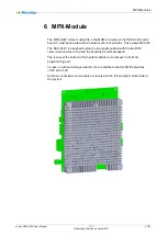
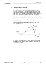
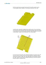

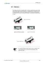
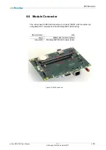


MPX-Module 6
miriac SBC-S32V User Manual
V 1.1
44/81
© MicroSys Electronics GmbH 2017
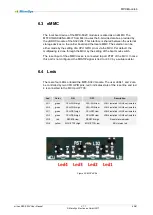
6.2
DRAM
The module is fitted with two individual DDR3L memory blocks, each 32bits wide
and with 1GByte capacity. The used parts are 4GBit devices organized in 256M x
16 bits with 15 row, 10 column and 3 bank addresses. The refresh rate depends on
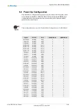
the operating temperature must be set according to the following table
Case Temperature
Refresh Cycle Time
Tc<85°C
7.8us
85°C<Tc<95°C
3.9us
95°C<Tc<105°C
1.95us
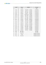
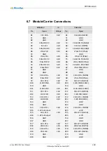
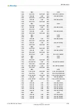
The DDR3L command bus is actively terminated and the routed in a fly by
structure. The following table shows all trace lengths, in case write leveling should
be adjusted. The used layer stack together with the FR4 material causes a signal
run time of 6.8ps/mm.
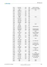
DRAM
Signal Group
Trace Length
Description
Bank0
Command
J1->J2
54.0mm
CPU->DRAM
Bank0
Command
J2->J3
13.1mm
DRAM->DRAM
Bank0
Byte 0
J1->J2
25.7mm
CPU->DRAM
Bank0
Byte 1
J1->J2
22.7mm
CPU->DRAM
Bank0
Byte 2
J1->J3
23.1mm
CPU->DRAM
Bank0
Byte 3
J1->J3
18.3mm
CPU->DRAM
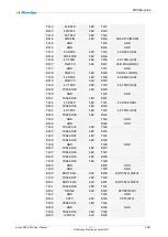
Bank1
Command
J1->J4
54.5mm
CPU->DRAM
Bank1
Command
J4>J5
13.9mm
DRAM->DRAM
Bank1
Byte 0
J1->J4
25.3mm
CPU->DRAM
Bank1
Byte 1
J1->J4
22.9mm
CPU->DRAM
Bank1
Byte 2
J1->J5
19.0mm
CPU->DRAM
Bank1
Byte 3
J1->J5
17.2mm
CPU->DRAM


