background image

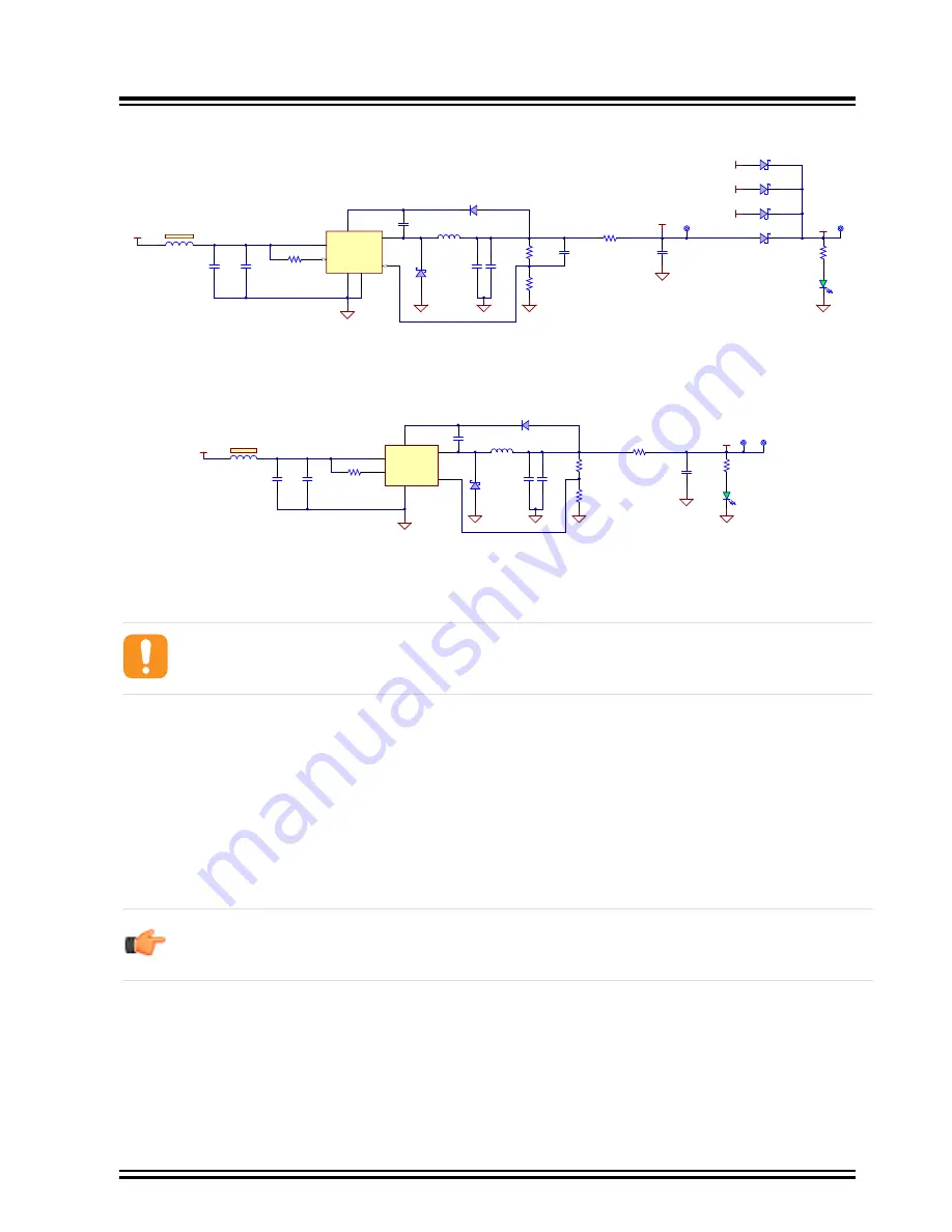
Figure 3-12. 5V Voltage Design

5V

GREEN

D9

GND

500mA max

5 Volts

VDC

GND

GND

GND

TP6

TP5

GND

0.1uF

C53

B140-13-F

D8

10uF

C56

10uF

C57

5V Buck Conver ter

470R

FB3

VBUS_JLINK

VUSB

22uH

L4

1N4448

D6

560R
0402

5%

R12

1M

R14

10k
0402
1%

R15

20pF
50V
0402

C54

6V to 48V

MBR0520

D7

MBR0520

D3

MBR0520

D4

5V_REG

5V_XPLAIN

MBR0520

D5

BOOST

7

GND

5

VFB

6

EN

2

SW

1

VIN

8

E

P

9

MCP16331

U2

1uF

C55

GND

0R

R11

10uF
75V
1210

C58

10uF
75V
1210

C59

56k
0402
1%

R13

Another buck converter, MC16301, is used to generate a regulated 3.3V voltage rail required by the PL485. For a
further description about the buck converter see the 

MCP16301/MCP16301H Datasheet

.

Figure 3-13. 3.3V Buck Converter Design

1

1

2

2

3

3

4

4

5

5

6

6

7

7

8

8

D

D

C

C

B

B

A

A

3 of 6

PL485 - Evaluation Kit

05/12/2019 15:01:59

Power Supply.SchDoc

Project Title

Sch #:

Date:

File:

Revision:

Sheet

Designed with

Drawn By:

JLCF

Sheet Title

Power Supply

Engineer:

JLCF

03-PL485

B

Size

A3

PL485-EK

PartNumber:

Variant Name

CEN-B

Altium.com

5V

GREEN

D9

GND

GND

500mA max

5 Volts

VDC

GND

GND

GND

TP6

TP5

TP4
TP7

GND

0.1uF

C53

B140-13-F

D8

10uF

C56

10uF

C57

5V Buck Conver ter

TP8

470R

FB3

3V3

GREEN

D12

GND

600mA max

3.3 Volts

5V

GND

GND

GND

TP10 TP11

GND

0.1uF

C60

B140-13-F

D11

10uF

C61

10uF

C62

15uH

L5

3V3 Buck Conver ter

TP9

470R

FB4

VBUS_JLINK

2

3

1

POWER 2.0mm

J3

VUSB

22uH

L4

1N4448

D6

1N4448

D10

560R
0402

5%

R12

52.3k
0402
1%

R13

1M

R14

1M

R19

300R

R18

10k
0402
1%

R15

10k
0402
1%

R20

31.6k
0402
1%

R17

20pF
50V
0402

C54

6V to 48V

MBR0520

D7

MBR0520

D3

MBR0520

D4

5V_REG

GND

VDC

TP3

0.1uF
100V
1206

C50

4.7uF
100V
1210

C49

SMBJ51A

D2

BOOST

1

GND

2

VFB

3

EN

4

SW

6

VIN

5

MCP16301T-I/CHY

U3

4.7uF
50V
1210

C64

4.7uF
50V
1210

C65

PMEG6010ER

D1

4A

F1

1
2

J2

PLC Connector

GND_IN

5V_XPLAIN

MBR0520

D5

Power Supply

560uH

L2

560uH

L3

0.1uF
100V
1206

C52

GND

GND_IN

BOOST

7

GND

5

VFB

6

EN

2

SW

1

VIN

8

E

P

9

MCP16331

U2

PLC+

PLC-

6V to 48V

1uF

C63

1uF

C55

GND

GND

0R

R16

0R

R11

0R

R9

0R

R10

50V

MOV1

10uF
75V
1210

C51

10uF
75V
1210

C58

10uF
75V
1210

C59

DC IN

DC Input

There is one LED and two test points on each voltage rail to check whether all power supplies are operating properly.

To avoid on board self-generated disturbances within the PLC signal band, both converters are switching at 500 kHz
fixed frequency, out of the PLC band (95 to 125 kHz).

Attention: 

 To avoid noise interferences, the switching frequency of the external SMPS must be out of the

PLC band and preferably in frequencies above it to avoid harmonics influence. This is essential to obtain a
good reception performance.

Please refer to section 

3.6  Hardware Description - JLINK Debugger

 for information about +3.3V LDO to supply J-

Link.

3.3.5.1 

PLC Rejection Filter

As the PLC coupling circuit is in parallel with the power supply circuit, the input impedance of the final equipment
could be affected. If the requirements about total input impedance are not satisfied, an appropriate input filter is
needed at the power supply input to increase the input impedance.

Besides the input filter, it is also recommended to add a PLC rejection filter to avoid the absorption of the PLC signals
by the power supply circuit. This filter also increases the input impedance, so it helps to achieve the requisites about
input impedance.

Notice: 

 The PL485-EK board has PLC coupling and power supply circuits in parallel, so the PLC

rejection filter is included. A PLC rejection filter is needed in case of low input impedance after connecting
in the same point the PLC Coupling connector J2 and the power source of the board.

The PLC rejection filter of the PL485-EK is composed of two inductors in-series (L = 560 μH) and a capacitor in-
parallel (C = 0.1 μF) at the power supply input as shown in the following picture.

 PL485-EK

PL485-EK Board

©

 2020 Microchip Technology Inc.

 User Guide

DS50002954B-page 19

Содержание PL485-EK

Страница 1: ...oard is shipped in an anti static shielding bag WARNING The board must not be subject to high electrostatic discharges It is recommended to use a grounding strap or similar ESD protective device when...

Страница 2: ...Xplained PRO PWR connector J7 DC Jack connector J3 or 2 position terminal block J2 Figure 1 PL485 EK Board top view PL485 EK 2020 Microchip Technology Inc User Guide DS50002954B page 2...

Страница 3: ...MCU Peripherals 20 3 5 Hardware Description MCU Interface Ports 21 3 6 Hardware Description JLINK Debugger 23 3 7 PL485 EK Schematics 27 3 8 PL485 EK Layout 32 4 Standards Compliance 36 5 References 3...

Страница 4: ...ponsibility for the consequences arising from an improper use of the PL485 EK board 1 2 Electrical Characteristics This section contains information about PL485 EK power supply requirements and consum...

Страница 5: ...smit a message which is received by the other end points in the network LED0 D19 green blinks to indicate that the application is running LED1 D20 red flashes when a PLC message is received and LED D1...

Страница 6: ...DC Input Connectors J2 J3 AC Coupler Connector J4 Xplained PRO PWR connector J7 ERASE Pin Header J1 CDC Disable Pin Header J13 JLINK Disable Pin Header J14 PL485 U1 JLINK USB Connector J12 JLINK 3 3V...

Страница 7: ...per Disable JLINK jumper Disable CDC jumper Interfaces USB Device mikroBUS Socket Connector SWD JTAG Debugging Port JLINK USB Embedded MPU Programmer Xplained PRO Master I2S Connector 3 2 1 PL485 EK B...

Страница 8: ...der J13 JLINK Disable Pin Header J14 JLINK USB Connector J12 PLC Signal and 3 2 2 1 Connectors The PL485 EK board includes the following connectors 1 PLC Connector and DC Input J2 same than J3 Table 3...

Страница 9: ...ADC Analog to digital converter alternatively a pin for the negative terminal of a differential ADC 5 PB10 GPIO1 General purpose I O 6 PB11 GPIO2 General purpose I O 7 PA0 PWM Pulse width Modulation a...

Страница 10: ...J8 Table 3 7 mikroBUS Socket Connector J8 Pin Signal Name Mnemonic Description 1 PA17 AN Analog 2 PA10 RST Reset 3 PA11 CS SPI Chip Select 4 PA14 SCK SPI Clock 5 PA12 MISO SPI Master Input Slave Outpu...

Страница 11: ...not have a series resistor 2 TMS SWDIO Serial Wire Input Output Test Mode Select JTAG mode set input of target CPU This pin should be pulled up on the target Typically connected to TMS of target CPU 3...

Страница 12: ...laced on the PL485 EK board for the verification of the main signals Table 3 12 Test Point Probes Reference Function TP6 5V TP8 GND TP9 GND TP10 3V3 TP16 PLC signal Table 3 13 Test Point Pads Referenc...

Страница 13: ...SB_N DUSB_P PL_NRST PL_CD PL_EXTIN PL_NPCS0 PL_SPCK PL_MOSI PL_MISO VDDIO H5 VDDIO A4 VDDIO B4 VDDIN_AN A5 VDDIN_AN B8 GND A1 VDDIO B10 PL_VDDCORE B11 VDDPLL C1 VDDPLL C2 PL_VDDCORE D1 VDDIN E1 VDDIO...

Страница 14: ...mikroBUS PB1 RXD6 UART_RX XPLAIN PB9 RXD4 XIN UART_RX mikroBUS PB2 TWCK1 I2C_SCL mikroBUS PB10 TXD4 DBGU_TX GPIO1 XPLAIN PB3 TWD1 I2C_SDA mikroBUS PB11 RXD4 DBGU_RX GPIO2 XPLAIN PB4 TDI TDI PB12 ERASE...

Страница 15: ...3 2 PLC Coupling Circuitry Description The PL485 EK evaluation board communicates in the band between 95 kHz and 125 kHz CENELEC B Band The PL485 EK board implements a circuit to couple the PLC signa...

Страница 16: ...rting the injected signal The filtering stage used in PL485 EK see Figure 3 7 has three aims Band pass filtering of high frequency components of the square waveform generated by the transmission stage...

Страница 17: ...402 R7 10k R8 0 1uF 25V 0402 C34 GND ADVREF GND 3V3 1R 0402 1 R6 4 7uF 10V 0402 C45 10uH L1 Near ball K7 1 3 20MHz Y1 PL_EMIT Balls connection D4 F3 E3 F2 E4 F4 E5 F5 E6 F6 E7 F7 E8 F8 G4 G5 G6 G7 Fig...

Страница 18: ...B_P USB_DP USB_DN USB Device 0R 0603 R3 R 03 1 1 2 J1 PB12 MCU slow clock MCU Erase MCU ERASE GND 1 4 2 3 TL3301NF260QG SW1 GND NRST MCU Reset 3V3 0 1uF C48 0R 0402 R2 0R 0402 R7 10k R8 0 1uF 25V 0402...

Страница 19: ...SW 1 VIN 8 EP 9 MCP16331 U2 PLC PLC 6V to 48V 1uF C63 1uF C55 GND GND 0R R16 0R R11 0R R9 0R R10 50V MOV1 10uF 75V 1210 C51 10uF 75V 1210 C58 10uF 75V 1210 C59 DC IN DC Input There is one LED and two...

Страница 20: ...tation of multiple functionalities such as Detection of fault conditions Detection of Low Power mode entering conditions Detection of wake up situations The input pin PA20 of PL485 is used to monitor...

Страница 21: ...if VUSBD is available Figure 3 17 USB Circuit 1 2 3 4 5 6 C B A I2S VUSBD GND GND GND GND PB14 USB_DP USB_DN USB Device USB_Device 1 2 3 4 5 0 ID D D 5V GND USB2 0MICRO BFEMALE J5 GND YELLOW D18 300R...

Страница 22: ...d pin out description in the Table 3 5 Figure 3 19 Xplained PRO Header Connector EXT1 1 2 3 4 5 6 D C B A Sch Drawn By JLCF Sheet Title Interface Engineer JLCF Size PL485 EK PartNumber 3V3 5 300 R58 I...

Страница 23: ...RO BFEMALE GND YELLOW D18 300R R40 4700pF C73 1 2 4 3 D17 PRTR5V0U2X GND GND 470R 470R FB12 5V Xplained PRO Socket 3V3 A23 A9 PB9 PB8 B2 B3 PA19 PB11 PA1 PA4 PB14 1 2 3 4 5 6 7 HDR 2 54 Male 1x7 J9 PA...

Страница 24: ...99 GND GND 3V3_3U 3V3 Connector for JT 3V3 GND 1 2 3 4 5 6 7 8 9 10 J15 VCC GND GND KEY GNDDetect PB1 PB0 PB6 PB7 PB5 PB4 PB11 PB10 TDI NC TDO SWO TCK SWCLK TMS SWDIO DBGU_TX DBGU_RX JLINK debugger JL...

Страница 25: ...NK_TMS_IN JLINK_nRST 100R 0402 1 R79 NRST JTAG_nRST 3V3 3V3 JTAG_CONN_TDI JTAG_CONN_TMS JTAG_CONN_TCK JTAG_CONN_TDO JTAG_CONN_nRST TRESIN TRESOUT JLINK_UART_RX JLINK_UART_TX JLINK_TDI_IN JLINK_TMS_IN...

Страница 26: ...D1_3U LED2_3U 2 1 4 3 GREEN RED 0805 D22 0402 R88 0402 R89 39R 0402 1 R86 39R 0402 1 R87 N P B2 1 GND 2 VCCA 3 A2 4 A1 5 OE 6 VCCB 7 B1 8 TXS0102 U8 22R 0402 1 R96 22R 0402 1 R98 0 1uF 10V 0402 C109 0...

Страница 27: ...IN PA16 NPCS02 SPI2_NCPS0 SPI_SS_A XPLAIN PA17 AD0 AD0 AN uBUS PA18 AD1 AD1 ADC XPLAIN PA19 AD2 AD2 ADC XPLAIN UserLed1 PA20 AD3 AD3 Voltage Monitor PA21 DM DUSB_N PA22 DP DUSB_P PA23 TIOA1 TIOA1 PWM...

Страница 28: ...3 C47 22pF 50v 0603 C46 PL_LDO_EN GND GND Clext 2x Ccrystal Cpara Cpcb Clext 2x 4 18 0 6 0 7 0 8 x Clext 2x 18 0 7 1 Clext 33 pF Pag 41 GND PL_XIN PL_XOUT PL_XOUT PL_XIN AGND 10000pF C1 0 022uF C4 0 0...

Страница 29: ...1 470R FB12 5V 3V3 GND Xplained PRO Header EXT1 VCC GND MISO SS SDA RXD GPIO PWM PWM GPIO2 GPIO1 ADC ADC GND ID SCK MOSI TXD 3V3 IRQ GPIO GND 1 2 3 4 5 6 7 8 9 10 11 12 13 14 15 16 17 18 19 20 HDR 2 5...

Страница 30: ...470R FB4 VBUS_JLINK 2 3 1 POWER 2 0mm J3 VUSB 22uH L4 1N4448 D6 1N4448 D10 560R 0402 5 R12 1M R14 1M R19 300R R18 10k 0402 1 R15 10k 0402 1 R20 31 6k 0402 1 R17 20pF 50V 0402 C54 6V to 48V MBR0520 D7...

Страница 31: ...R34 3 1 2 DM N2056U Q3 3 1 2 DM N2056U Q1 510R 0603 R27 0R R28 1 2 3 BAT54SLT1 D13 10k R26 10k R21 GND 3V3 22uH L6 2 2uH L8 15uH L7 1uF 25V 0805 C68 0 15uF 50V 1206 C67 3 3R 0805 1 R24 0R R23 1 2 3 4...

Страница 32: ...CONN_TCK JTAG_CONN_TDO S 1 I0A 2 I1A 3 YA 4 I0B 5 I1B 6 YB 7 GND 8 YC 9 I1C 10 I0C 11 YD 12 I1D 13 I0D 14 E 15 VCC 16 IDTQS3VH257PAG U4 100k 0402 5 R70 3 1 2 BSS138N Q4 DIS_JLINK JLINK_TCK_IN JLINK_TD...

Страница 33: ...Figure 3 35 PL485 EK rev1 Layout Top Layer Figure 3 36 PL485 EK rev1 Layout Mid Layer 1 Ground PL485 EK PL485 EK Board 2020 Microchip Technology Inc User Guide DS50002954B page 33...

Страница 34: ...Figure 3 37 PL485 EK rev1 Layout Mid Layer 2 Power Supplies Figure 3 38 PL485 EK rev1 Layout Bottom Layer PL485 EK PL485 EK Board 2020 Microchip Technology Inc User Guide DS50002954B page 34...

Страница 35: ...Figure 3 39 PL485 EK rev1 Layout Top Silkscreen Figure 3 40 PL485 EK rev1 Layout Bottom Silkscreen PL485 EK PL485 EK Board 2020 Microchip Technology Inc User Guide DS50002954B page 35...

Страница 36: ...appliance nor is it intended for incorporation into finished appliances that are made commercially available as single functional units to end users The PL485 EK board is a CE mark product which compl...

Страница 37: ...et 2020 PLC AC Coupler User Guide 2020 Using PL485 to implement a fully featured G3 PLC PRIME modem Application Note 2020 MCP16331 High Voltage Input Buck Converter Evaluation Board User s Guide 2014...

Страница 38: ...3 1 PL485 section Deleted note in 3 3 2 PLC Coupling Circuitry Description section Added reference to PLC AC Coupler User Guide in 3 3 2 2 PLC Coupling Circuit section Updated 3 3 3 Clock Circuitry s...

Страница 39: ...is available through the website at http www microchip com support Microchip Devices Code Protection Feature Note the following details of the code protection feature on Microchip devices Microchip p...

Страница 40: ...Plus ProASIC Plus logo Quiet Wire SmartFusion SyncWorld Temux TimeCesium TimeHub TimePictra TimeProvider Vite WinPath and ZL are registered trademarks of Microchip Technology Incorporated in the U S A...

Страница 41: ...7252 China Xiamen Tel 86 592 2388138 China Zhuhai Tel 86 756 3210040 India Bangalore Tel 91 80 3090 4444 India New Delhi Tel 91 11 4160 8631 India Pune Tel 91 20 4121 0141 Japan Osaka Tel 81 6 6152 7...

Отзывы: