Pin No. Mnemonic
Type
Description
13
RXC_2−
HDMI input
Digital Input Channel 2 Complement of Port C in the HDMI Interface.
14
RXC_2+
HDMI input
Digital Input Channel 2 True of Port C in the HDMI Interface.
15
HP_CTRLD
Digital output
Hot Plug Detect for Port D.
16
5V_DETD
Digital input
5 V Detect Pin for Port D in the HDMI Interface.
17
DGND
Ground
DVDD Ground.
18
DVDD
Power
Digital Supply Voltage (1.8 V).
19
DDCD_SDA
Digital I/O
HDCP Slave Serial Data Port D. DDCD_SDA is a 3.3 V input/output that is 5 V tolerant.
20
DDCD_SCL
Digital input
HDCP Slave Serial Clock Port D. DDCD_SCL is a 3.3 V input that is 5 V tolerant.
21
CVDD
Power
Receiver Comparator Supply Voltage (1.8 V).
22
CGND
Ground
TVDD and CVDD Ground.
23
RXD_C−
HDMI input
Digital Input Clock Complement of Port D in the HDMI Interface.
24
RXD_C+
HDMI input
Digital Input Clock True of Port D in the HDMI Interface.
25
TVDD
Power
Receiver Terminator Supply Voltage (3.3 V).
26
RXD_0−
HDMI input
Digital Input Channel 0 Complement of Port D in the HDMI Interface.
27
RXD_0+
HDMI input
Digital Input Channel 0 True of Port D in the HDMI Interface.
28
CGND
Ground
TVDD and CVDD Ground.
29
RXD_1−
HDMI input
Digital Input Channel 1 Complement of Port D in the HDMI Interface.
30
RXD_1+
HDMI input
Digital Input Channel 1 True of Port D in the HDMI Interface.
31
TVDD
Power
Receiver Terminator Supply Voltage (3.3 V).
32
RXD_2−
HDMI input
Digital Input Channel 2 Complement of Port D in the HDMI Interface.
33
RXD_2+
HDMI input
Digital Input Channel 2 True of Port D in the HDMI Interface.
34
CVDD
Power
Receiver Comparator Supply Voltage (1.8 V).
35
CGND
Ground
TVDD and CVDD Ground.
36
TXPVDD
Power
1.8 V Power Supply for Digital and I/O Power Supply. This pin supplies power to the
digital logic and I/Os. It should be filtered and as quiet as possible.
37
TXPLVDD
Power
1.8 V Power Supply.
38
TXGND
Ground
TXPVDD Ground.
39
TXPGND
Ground
TXPLVDD Ground.
40
EXT_SWING
Analog input
This pin sets the internal reference currents. Place an 887 Ω resistor (1% tolerance) between
this pin and ground.
41
HPD_ARC−
Analog input
Hot Plug Detect Signal. This pin indicates to the interface whether the receiver is connected.
It supports 1.8 V to 5 V CMOS logic levels.
42
ARC+
Analog input
Audio Return Channel Input (5 V Tolerant).
43
TXDDC_SDA Digital I/O
Serial Port Data I/O to Receiver. This pin serves as the master to the DDC bus. It supports a
5 V CMOS logic level.
44
TXDDC_SCL
Digital output
Serial Port Data Clock to Receiver. This pin serves as the master clock for the DDC bus.
It supports a 5 V CMOS logic level.
45
TXAVDD
Power
1.8 V Power Supply for TMDS Outputs.
46
TXGND
Ground
TXAVDD Ground.
47
TXC−
HDMI output
Differential Clock Output. Differential clock output at the TMDS clock rate; supports
TMDS logic level.
48
TXC+
HDMI output
Differential Clock Output. Differential clock output at the TMDS clock rate; supports
TMDS logic level.
49
TXGND
Ground
TXAVDD Ground.
50
TX0−
HDMI output
Differential Output Channel 0 Complement. Differential output of the red data at 10×
the pixel clock rate; supports TMDS logic level.
51
TX0+
HDMI output
Differential Output Channel 0 True. Differential output of the red data at 10× the pixel clock
rate; supports TMDS logic level.
52
TXGND
Ground
TXAVDD Ground.
53
TX1−
HDMI output
Differential Output Channel 1 Complement. Differential output of the red data at 10×
the pixel clock rate; supports TMDS logic level.
54
TX1+
HDMI output
Differential Output Channel 1 True. Differential output of the red data at 10× the pixel
clock rate; supports TMDS logic level.
55
TXAVDD
Power
1.8 V Power Supply for TMDS Outputs.
137
Содержание NR1504 /U1B
Страница 9: ...Personal notes 9 ...
Страница 144: ...W9864G6JH 6 DIGITAL U1005 W9864G2IH Publication Release Date Aug 28 2009 4 Revision A03 4 PIN CONFIGURATION 144 ...
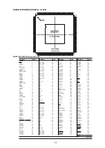
Страница 162: ...2 FL DISPLAY FLD 018BT021GINK FRONT U4400 PIN CONNECTION GRID ASSIGNMENT 162 ...
Страница 163: ...ANODE CONNECTION 163 ...


