5
6
QF01
: µ
: µ
: µ
: µ
: µ
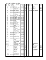
PD78076 MAIN
SYMBOL
PIN
PADCELL
DESCRIPTION
RC
fil
1
E029
PLL loop filter input
V
ref
2
E029
decoupling internal reference voltage output
V
DDA
3
E008
analog supply voltage
V
SSA
4
E004
analog ground
IECIN1
5
E007
high sensitivity IEC input
IECIN0
6
IPP04
TTL level IEC input
IECSEL
7
IUP04
select IEC input 0 or 1 (0 = IECIN0; 1 = IECIN1); this input has an internal pull-up
resistor
IECO
8
OPFH3
digital audio output for optical and transformer link
IECOEN
9
IUP04
digital audio output enable (0 = enabled; 1 = disabled/3-state); this input has an
internal pull-up resistor
TESTB
10
IPP04
enable factory test input (0 = normal application; 1 = scan mode)
TESTC
11
IPP04
enable factory test input (0 = normal application; 1 = observation outputs)
UNLOCK
12
OPP41A
PLL out-of-lock (0 = not locked; 1 = locked); this output can drive an LED
FS32
13
OPP41A
indicates sample frequency = 32 kHz (active LOW); this output can drive an LED
FS44
14
OPP41A
indicates sample frequency = 44.1 kHz (active LOW); this output can drive an LED
FS48
15
OPP41A
indicates sample frequency = 48 kHz (active LOW); this output can drive an LED
CHMODE
16
OPP41A
use of channel status block (0 = professional use; 1 = consumer use); this output
can drive an LED
V
DDD2
17
E008
digital supply voltage 2
V
SSD2
18
E009
digital ground 2
RESET
19
IDP09
initialization after power-on, requires only an external capacitor connected to V
DDD
;
this is a Schmitt-trigger input with an internal pull-down resistor
PD
20
IPP04
enable power-down input in the standby mode (0 = normal application; 1 = standby
mode)
CTRLMODE
21
IUP04
select microcontroller/stand-alone mode (0 = microcontroller; 1 = stand-alone); this
input has an internal pull-up resistor
LADDR
22
IPP04
microcontroller interface address switch input (0 = 000001; 1 = 000010)
LMODE
23
IPP09
microcontroller interface mode line input
LCLK
24
IPP09
microcontroller interface clock line input
LDATA
25
IOF24
microcontroller interface data line input/output
STROBE
26
IDP04
strobe for control register (active HIGH); this input has an internal pull-down resistor
UDAVAIL
27
OPF23
synchronization for output user data (0 = data available; 1 = no data)
TESTA
28
IPP04
enable factory (scan) test input (0 = normal application; 1 = test clock enable)
COPY
29
OPP41A
copyright status bit (0 = copyright asserted; 1 = no copyright asserted); this output
can drive an LED
INVALID
30
IOD24
validity of audio sample input/output (0 = valid sample; 1 = invalid sample); this pin
has an internal pull-down resistor
DEEM
31
OPF23
pre-emphasis output bit (0 = no pre-emphasis; 1 = pre-emphasis)
MUTE
32
IUP04
audio mute input (0 = permanent mute; 1 = mute on receive error); this pin has an
internal pull-up resistor
I
2
SSEL
33
IUP04
select auxiliary input or normal input in transmit mode
SDAUX
34
IPP04
auxiliary serial data input; I
2
S-bus
SD
35
IOF24
serial audio data input/output; I
2
S-bus
WS
36
IOF24
word select input/output; I
2
S-bus
SCK
37
IOF29
serial audio clock input/output; I
2
S-bus
I
2
SOEN
38
IUP04
serial audio output enable (0 = enabled; 1 = disabled/3-state); this input has an
internal pull-up resistor
SYSCLKI
39
IPP09
system clock input (transmit mode)
SYSCLKO
40
OPFA3
system clock output (receive mode)
V
SSD1
41
E009
digital ground 1
V
DDD1
42
E008
digital supply voltage 1
CLKSEL
43
IUP04
select system clock (0 = 384f
s
; 1 = 256f
s
); this input has an internal pull-up resistor
RC
int
44
E029
integrating capacitor output
Q507/Q509 : DSP56004
QD03/QD53 : TDA1541A/S2
Q304 : TDA1315H
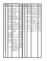
Pin No. Port Name Function In/Out Active
To/From
Description
1
STRB
P120
Out
High
Q304
Strobe signal for control resister for Q304(TDA1315H)
2
LMOD
P121
Out
Low
Q304
Interface mode line for Q304(TDA1315H)
3
OPEN
P122
-----
4
GND
P123
GND
GND
5
FS32
P124
In
Low
Q304
Sampling frequency input (L = 32KHz Receiving)
6
FS48
P125
In
Low
Q304
Sampling frequency input (L = 48KHz Receiving)
7
COAX/OPT P126
Out
Low
Q304
Digital input select signal (L = Optical , H = Coaxal)
8
DMUT
P127
Out
Low
Q304
Digital muting control signal for Q304(TDA1315H)
9
GND
IC
GND
GND
10
5MHzXTAL
X2
XF01
Clock out (5MHz)
11
5MHzXTAL
X1
XF01
Clock in (5MHz)
12
+5V
Vdd
+5V
Power 5V
13
OPEN
XT2
---
-----
14
+5V
XT1
+5V
Power 5V
15
REST
RESET
In
Low
QF02
Reset signal input for QF02
16
RC5I
INTP0
In
ZY01
Remote control signal input for ZY01
17
OPEN
INTP1
---
-----
18
CD7R
P02
Out
Low
Q102
CD7 Reset signal for Q102(SAA7372GP)
19
SILD
P03
Out
Low
Q102
Strobe signal for servo part of Q102(SAA7372GP)
20
RAB7
P03
Out
Low
Q102
Strobe signal for digital part of Q102(SAA7372GP)
21
LOCK
INTP5
In
Low
Q304
Unlock signal of Q304(TDA1315H)
22
MSCP
INTP6
In
Low
GND
GND
23
+5V
Avdd
+5V
Power 5V
24
+5V
Avref0
In
+5V
Power 5V
25
KEY0
ANI0
In
Level Tact Switch Key Sensor
26
KEY1
ANI1
In
Level Tact Switch Key Sensor
27
KEY2
ANI2
In
Level Tact Switch Key Sensor
28
GND
ANI3
GND
GND
29
MUTE
ANI4
Out
High
Q507
Mute signal for DSP Q507(DSP56004)
30
PAUS
ANI5
Out
High
Q507
Mute of pause on time for DSP Q507(DSP56004)
31
OPEN
ANI6
(CD7L)
-----
32
RELY2
ANI7
Out
High
QY51
Display on/off control signal (L = off , H = on)
33
GND
Avss
GND
GND
34
OPEN
P130 In/Out
---
-----
35
OPEN
P131
Out
---
-----
36
+5V
Avref
In
+5V
Power 5V
37
STRD
P70
Out
Low
QY01
Strobe signal for QY01
38
SIOD
SO2
Out
QY01
Serial data for QY01
39
CLKD
SCK2
Out
Low
QY01
Serial clock for QY01
40
GND
Vss
GND
GND
41
OPEN
SI1
In
---
-----
42
OPEN
SO1
---
-----
43
OPEN
SCK1
---
-----
44
OPEN
P23
-----
45
OPEN
P24
---
-----
46
OPEN
SB0
-----
47
OPEN
SB1
In/Out
---
-----
48
SDA
SCK0
Out
Q102/Q304 Serial data signal for Q102/Q304
49
SCL
A0
Q102/Q304 Serial clock signal for Q102/Q304
50
OPEN
A1
---
-----
51
OPEN
A2
---
-----
52
OPEN
A3
---
-----
53
OPEN
A4
---
-----
54
OPEN
A5
---
-----
55
OPEN
A6
---
-----
56
OPEN
A7
---
-----
57
GND
D0
GND
58
GND
D1
GND
59
GND
D2
GND
60
GND
D3
GND
61
GND
D4
GND
62
GND
D5
GND
63
GND
D6
GND
64
GND
D7
GND
GND
GND
GND
GND
GND
GND
GND
GND
65
OPEN
A8
---
-----
66
OPEN
A9
---
-----
67
OPEN
A10
---
-----
68
OPEN
A11
---
-----
69
OPEN
A12
---
-----
70
OPEN
A13
---
-----
71
GND
Vss
GND
GND
72
OPEN
A14
(RA12)
-----
73
RA11
A15
Out
High
Q506
Audio data select signal output (L = 16Bit)
74
16WD
P60
In
Low
GND
Audio data select signal input (L = 16Bit)
75
FMUT
P61
Out
High
QN05
Mute of switching on time killer
76
RSD2
P62
Out
Low Q309,Q509 Reset of Q309,Q509
77
RSD1
P63
Out
Low
Q507
Reset of Q507
78
NSSH
RD
Out
Low Q508,QY10 Noise shaper on/off signal (L = on , H = off)
79
FIL3
WR
Out
High Q508,QY09 Filter 3 select signal (H = select of filter 3)
80
FIL2
P66
Out
High Q508,QY08 Filter 2 select signal (H = select of filter 2)
81
FIL1
P67
Out
High
QY07
Filter 1 select signal (H = select of filter 1)
82
OPTI
P100
In
High
Q303
Optical input select ( H = OPT , L = COAX1)
83
OPEN
TO6
---
-----
84
OPEN
P102
---
-----
85
RELY1
P103
Out
High
D301
Audio muting control signal of poer on/off(H=mute on)
86
MSL1
P30
In
High High Level -----
87
MSL2
P31
In
Low GND Level -----
88
OPEN
P32
---
-----
89
CDRW
P33
Out
High
NC
-----
90
SLSW
P34
In
Low
VAM1201 Sledge detect switch (L = in end)
91
TROS
P35
In
Low
TRAY
Tray in/out detect switch (L = out end)
92
TRIS
P36
In
Low
TRAY
Tray in/out detect switch (L = in end)
93
TRUS
P37
In
Low
TRAY
Tray up/down detect switch (L = up end)
94
TRDS
P90
In
Low
TRAY
Tray up/down detect switch (L = down end)
95
TROM
P91
Out
High
QM10
Tray motor control signal (H = tray out)
96
TRIM
P93
Out
High
QM09
Tray motor control signal (H = tray in)
97
TRDM
P94
Out
High
QM12
Tray motor control signal (H = tray down)
98
TRUM
P95
Out
High
QM11
Tray motor control signal (H = tray up)
99
AMUT
P95
Out
Low
NC
-----
100
DA/CD
P96
Out
Low
Q504
Mode select (L = D/A Mode , H = CD Mode)
---
---
PINNING
Note
1. See Table 1 data selection input.
SYMBOL
PIN
DESCRIPTION
LE/WS
(1)
1
latch enable input/ word select
input
BCK
(1)
2
bit clock input
DATA L
/DATA
(1)
3
data left channel input/ data
input (selected format)
DATA R
(1)
4
data right channel input
GND(A)
5
analog ground
AOR
6
right channel output
DECOU
7 to 13
decoupling
GND (D)
14
digital ground
V
DD2
15
−
15 V supply voltage
COSC
16,17
oscillator
DECOU
18 to 24 decoupling
AOL
25
left channel output
V
DD1
26
−
5 V supply voltage
OB/TWC
(1)
27
mode select input
V
DD
28
+5 V supply voltage
Y Data
Memory*
X Data
Memory*
Program
Memory*
Program Control Unit
24-Bit
DSP56000
Core
OnCETM Port
PLL
Clock
Gen.
4
9
5
29
16-Bit Bus
24-Bit Bus
Interrupt
Control
4
IRQA
, IRQB, NMI, RESET
4
3
Address
Generation
Unit
PAB
XAB
YAB
GDB
PDB
XDB
YDB
General
Purpose
Input/
Output
External
Memory
Interface
(EMI)
Serial
Audio
Interface
(SAI)
Serial
Host
Interface
(SHI)
*Refer to Table 1 for memory configurations.
Internal
Data
Bus
Switch
Program
Decode
Controller
Program
Address
Generator
Data ALU
24
×
24 + 56
→
56-bit MAC
Two 56-Bit Accumulators
MA0ÐMA14
MD0ÐMD7
MWR
MA17/MCS1/MRAS
MA16/MCS2/MCAS
GND
Q
V
CCQ
RESET
MODA/IRQA
MODB/IRQB
MODC/NMI
SS/HA2
MISO/SDA
SCK/SCL
GND
S
V
CCS
WSR
SCKR
SDI0
DSCK/OS1
DSI/OS0
DSO
DR
OnCEª
Port C
Port B
Port A
External Memory
Mode/Interrupt
80 signals
Serial Host
Rec0
SDO1
Tran1
WST
SCKT
SDO0
Tran0
Interface
MRD
MCS0
Serial Audio
Interface
Interface
MOSI/HA0
SDO2
Tran2
SDI1
Rec1
GPIO0ÐGPIO3
GPIO
HREQ
V
CCP
GND
P
PCAP
PLL
PINIT
MA15/MCS3
EXTAL
GND
A
V
CCA
GND
D
V
CCD
Reset
Port
Power Inputs
Ground
Control
2
2
3
3
4
2
3
8
4
15
DSP56004
Содержание 74 CD7
Страница 8: ...7 8 6 WIRING DIAGRAM ...
Страница 10: ...9 SCHEMATIC DIAGRAM AND PARTS LOCATION 11 12 ...
Страница 11: ...13 14 ...
Страница 12: ...15 16 ...
Страница 13: ...17 18 ...
Страница 14: ...19 20 ...


