
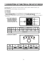
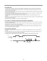
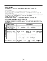
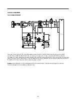
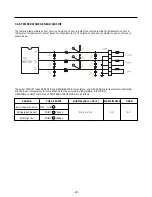
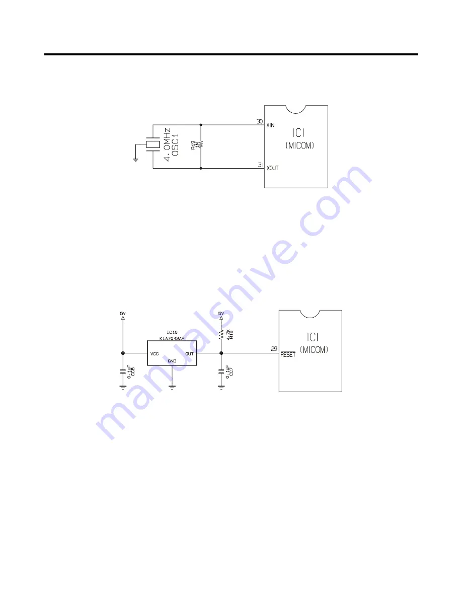
7-2-2 OSCILLATION CIRCUIT
This circuit is to generate the base clock for calculating time and the synchro clock for transmitting data from and to the
inside logic elements of the IC1(MICOM). Be sure to use the authentic parts since the calculating time by the IC1 may be
changed or it will not work if the OSC1 SPEC is changed.
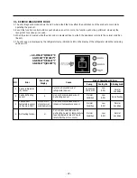
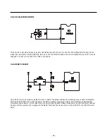
7-2-3 RESET CIRCUIT
The RESET circuit is for allowing all the functions to start at the initial conditions by initializing various parts including the
RAM inside the MICOM (IC1) when the power is initially supplied or the power supply to the MICOM is restored after a
momentary power failure. For the initial 10ms of power supply, ÔLOWÕ voltage is applied to the MICOM RESET terminal.
During a normal operation, 5V is applied to the RESET terminal. (If a trouble occurs in the RESET IC, the MICOM will not
work.)
- 26 -
Содержание B712Y*B
Страница 36: ...7 5 2 REPLACEMENT PARTS LIST 36 ...
Страница 37: ... 37 ...
Страница 38: ...7 5 3 PWB ASS Y DISPLAY AND PARTS LIST 38 ...
Страница 39: ... 39 7 5 4 PWB ASS Y DISPLAY I MICOM AND PARTS LIST ...
Страница 40: ... 40 7 5 5 V LED DISPLAY PART LIST ...
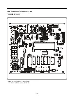
Страница 41: ...7 6 PWB DIAGRAM 41 ...
Страница 42: ... 42 ...
Страница 44: ... 44 149D 155J 149B 120 118 119 138 120 110 111 149B 405A 140A 133 405C 405C 404A ...
Страница 45: ... 45 101 122 241D 244C 244A 162 212C 212A 205A 241A 279A 123 102 241C 235A 205A 210A 173 172 241E ...
Страница 46: ...P No MFL38971701 MAR 2007 Printed in Korea ...


